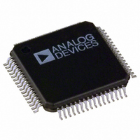
AD7656YSTZ Analog Devices Inc, AD7656YSTZ Datasheet - Page 29

AD7656YSTZ
Manufacturer Part Number
AD7656YSTZ
Description
IC ADC 16BIT 6CH 250KSPS 64LQFP
Manufacturer
Analog Devices Inc
Datasheet
1.AD7656BSTZ-500RL7.pdf
(32 pages)
Specifications of AD7656YSTZ
Data Interface
Serial, Parallel
Number Of Bits
16
Sampling Rate (per Second)
250k
Number Of Converters
6
Power Dissipation (max)
143mW
Voltage Supply Source
Analog and Digital, Dual ±
Operating Temperature
-40°C ~ 125°C
Mounting Type
Surface Mount
Package / Case
64-LQFP
Resolution (bits)
16bit
Sampling Rate
250kSPS
Input Channel Type
Single Ended
Supply Voltage Range - Digital
4.75V To 5.25V
Supply Current
26mA
Lead Free Status / RoHS Status
Lead free / RoHS Compliant
For Use With
EVAL-AD7656-1EDZ - BOARD EVAL CONTROL AD7656-1EVAL-AD7656-1CBZ - BOARD EVAL FOR AD7656-1EVAL-AD7656CBZ - BOARD EVAL FOR AD7656
Lead Free Status / RoHS Status
Lead free / RoHS Compliant, Lead free / RoHS Compliant
Available stocks
Company
Part Number
Manufacturer
Quantity
Price
Company:
Part Number:
AD7656YSTZ
Manufacturer:
Analog Devices Inc
Quantity:
10 000
Company:
Part Number:
AD7656YSTZ-1
Manufacturer:
Analog Devices Inc
Quantity:
10 000
Part Number:
AD7656YSTZ-1
Manufacturer:
ADI/亚德诺
Quantity:
20 000
Company:
Part Number:
AD7656YSTZ-1-RL
Manufacturer:
Analog Devices Inc
Quantity:
10 000
Company:
Part Number:
AD7656YSTZ-REEL
Manufacturer:
Analog Devices Inc
Quantity:
10 000
APPLICATION HINTS
LAYOUT
The printed circuit board that houses the AD7656/AD7657/
AD7658 should be designed so that the analog and digital
sections are separated and confined to certain areas of the board.
At least one ground plane should be used. It could be common
or split between the digital and analog sections. In the case of
the split plane, the digital and analog ground planes should be
joined in only one place, preferably underneath the AD7656/
AD7657/AD7658, or at least as close as possible to each part.
If the AD7656/AD7657/AD7658 are in a system where multiple
devices require analog-to-digital ground connections, the
connection should still be made at only one point, a star ground
point, which should be established as close as possible to the
AD7656/AD7657/AD7658. Good connections should be made
to the ground plane. Avoid sharing one connection for multiple
ground pins. Individual vias or multiple vias to the ground
plane should be used for each ground pin.
Avoid running digital lines under the devices because doing so
couples noise onto the die. The analog ground plane should be
allowed to run under the AD7656/AD7657/AD7658 to avoid
noise coupling. Fast-switching signals like CONVST or clocks
should be shielded with digital ground to avoid radiating noise
to other sections of the board, and they should never run near
analog signal paths. Crossover of digital and analog signals
should be avoided. Traces on different but close layers of the
board should run at right angles to each other to reduce the
effect of feedthrough through the board.
The power supply lines to the AV
pins on the AD7656/AD7657/AD7658 should use as large a
trace as possible to provide low impedance paths and reduce the
effect of glitches on the power supply lines. Good connections
should be made between the AD7656/AD7657/AD7658 supply
pins and the power tracks on the board; this should involve the
use of a single via or multiple vias for each supply pin.
CC
, DV
CC
, V
DRIVE
, V
DD
, and V
Rev. A | Page 29 of 32
SS
Good decoupling is also important to lower the supply
impedance presented to the AD7656/AD7657/AD7658 and to
reduce the magnitude of the supply spikes. Decoupling ceramic
capacitors, typically 100 nF, should be placed on all of the power
supply pins, V
capacitors should be placed close to, ideally right up against,
these pins and their corresponding ground pins. Additionally,
low ESR 10 μF capacitors should be placed on each of the
supply pins. Avoid sharing these capacitors between pins. Use
big vias to connect the capacitors to the power and ground
planes. Use wide, short traces between the via and the capacitor
pad, or place the via adjacent to the capacitor pad to minimize
parasitic inductances. Recommended decoupling capacitors are
100 nF, low ESR, ceramic capacitors (Farnell 335-1816) and
10 μF, low ESR, tantalum capacitors (Farnell 197-130) for the
AV
be placed where the AV
An alternative reduced decoupling arrangement is outlined in
the Typical Connection Diagram section. This decoupling
arrangement groups the AV
the decoupling capacitors to be shared between the supply pairs.
Group the six AV
Pin 35, Pin 40 and Pin 41, and Pin 46 and Pin 47. Connect the
supply pins in each pair together; their location on the AD7656/
AD7657/AD7658 pin configuration easily facilitates this. For
the AD7656, decouple each pair with a 100 μF capacitor; for the
AD7657, decouple each pair with a 33 μF capacitor; for the
AD7658, decouple each pair with a 22 μF capacitor. For this
minimum decoupling configuration, all other supply and
reference pins should be decoupled with a 10 μF decoupling
capacitor.
CC
decoupling. A large tantalum decoupling capacitor should
DD
, V
CC
SS
core supply pins into three pairs, Pin 34 and
, AV
CC
AD7656/AD7657/AD7658
CC
supply enters the board.
, DV
CC
supply pins into pairs and allows
CC
, and V
DRIVE
. These decoupling


