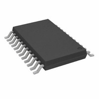
AD7739BRU Analog Devices Inc, AD7739BRU Datasheet - Page 30

AD7739BRU
Manufacturer Part Number
AD7739BRU
Description
IC ADC 24BIT 8-CH 24-TSSOP
Manufacturer
Analog Devices Inc
Datasheet
1.AD7739BRUZ.pdf
(32 pages)
Specifications of AD7739BRU
Rohs Status
RoHS non-compliant
Number Of Bits
24
Sampling Rate (per Second)
15.1k
Data Interface
DSP, MICROWIRE™, QSPI™, Serial, SPI™
Number Of Converters
1
Power Dissipation (max)
100mW
Voltage Supply Source
Analog and Digital
Operating Temperature
-40°C ~ 105°C
Mounting Type
Surface Mount
Package / Case
24-TSSOP (0.173", 4.40mm Width)
For Use With
EVAL-AD7739EBZ - BOARD EVAL FOR AD7739
Available stocks
Company
Part Number
Manufacturer
Quantity
Price
Company:
Part Number:
AD7739BRUZ
Manufacturer:
ADI
Quantity:
1 000
Company:
Part Number:
AD7739BRUZ
Manufacturer:
Analog Devices Inc
Quantity:
1 859
Part Number:
AD7739BRUZ
Manufacturer:
ADI/亚德诺
Quantity:
20 000
Company:
Part Number:
AD7739BRUZ-REEL7
Manufacturer:
ADI
Quantity:
1 000
AD7739
CALIBRATION
The AD7739 provides zero-scale self-calibration, and zero- and
full-scale system calibration capability that can effectively
reduce the offset error and gain error to the order of the noise.
After each conversion, the ADC conversion result is scaled
using the ADC calibration registers and the relevant channel
calibration registers before being written to the data register.
For unipolar ranges:
Data = ((ADC result – R × ADC ZS Cal. reg.)
For bipolar ranges:
Data = ((ADC result – R × ADC ZS Cal. reg.)
where the ADC result is in the range of 0 to 0xFF FFFF.
R = 1 for input ranges +1.25 V, ±1.25 V, +2.5 V, and ±2.5 V
R = 2 for input ranges +0.625 V, and ±0.625 V
Note that the channel zero-scale calibration register has the
format of a sign bit and a 22-bit channel offset value.
To start any calibration, write the relevant mode bits to the
AD7739 mode register. After the calibration is complete, the
contents of the corresponding calibration registers are updated,
all RDY bits in the ADC status register are set, the SYNC pin
goes low, and the AD7739 reverts to idle mode. The calibration
duration is the same as the conversion time configured on the
selected channel. A longer conversion time gives less noise and
yields a more exact calibration; therefore, use at least the default
conversion time to initiate any calibration.
ADC Zero-Scale Self-Calibration
The ADC zero-scale self-calibration can reduce the ADC offset
error in the chopping disabled mode. If repeated after a
temperature change, it can also reduce the offset drift error in
the chopping disabled mode.
The zero-scale self-calibration is performed on internally
shorted ADC inputs. The negative analog input terminal on the
selected channel is used to set the ADC zero-scale calibration
common mode. Therefore, either the negative terminal of the
selected differential pair or the AINCOM on the single-ended
channel configuration should be driven to a proper common-
mode voltage.
It is recommended that the ADC zero-scale calibration register
be updated only as part of an ADC zero-scale self-calibration.
× ADC FS reg./(0x20 0000) – R × Ch. ZS Cal. reg.)
× ADC FS reg./(0x40 0000) + (0x80 0000) – R × Ch. ZS Cal. reg.)
× Ch. FS Cal. reg./(0x20 0000)
× Ch. FS Cal. reg./(0x20 0000)
Rev. 0 | Page 30 of 32
ADC Full-Scale Self-Calibration
The ADC full-scale self-calibration can reduce the ADC full-
scale error for the +2.5 V and ±2.5 V input range. If repeated
after a temperature change, it can also reduce the full-scale drift.
The ADC full-scale self-calibration is performed with a +2.5 V
input voltage range on internally generated full-scale voltage
(V
setup register. Full-scale errors in the ±1.25 V, +1.25 V, ±0.625 V,
and +0.625 V ranges are not calibrated as this would require an
accurate low voltage source other than the reference.
If the 1.25 V or 0.625 V ranges are used on any channel, the
ADC full-scale self-calibration is not recommended. A system
full-scale calibration should be performed if accurate gains
need to be achieved on these ranges.
It is recommended that the ADC full-scale calibration register
be updated only as part of an ADC full-scale self-calibration for
the +2.5 V and ±2.5 V input range.
Per Channel System Calibration
The per channel system calibration can reduce the system offset
error and the system gain error. If repeated after a temperature
change, it can also reduce the system offset and gain drifts.
If the per channel system calibrations are used, these should be
initiated in the following order: a channel zero-scale system
calibration, followed by a channel full-scale system calibration.
The system calibration is affected by the ADC zero-scale and
full-scale calibration registers. Therefore, if both self-calibration
and system calibration are used in the system, an ADC self-
calibration should be performed first, followed by a system
calibration cycle.
The voltage range in the channel setup register should be set
before executing the channel system calibration.
While executing a system calibration, the fully settled system
zero-scale voltage signal or system full-scale voltage signal must
be connected to the selected channel analog inputs.
The per channel calibration registers can be read, stored, or
modified and written back to the AD7739. Note that when
writing the calibration registers, the AD7739 must be in idle
mode. Note that outside the specified calibration range,
calibration is possible, but the performance may degrade
(see the System Calibration section in Table 1).
REF
), regardless of the input voltage range set in the channel


