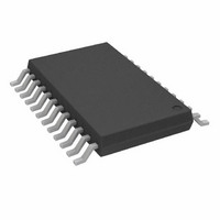
AD7739BRU Analog Devices Inc, AD7739BRU Datasheet - Page 15

AD7739BRU
Manufacturer Part Number
AD7739BRU
Description
IC ADC 24BIT 8-CH 24-TSSOP
Manufacturer
Analog Devices Inc
Datasheet
1.AD7739BRUZ.pdf
(32 pages)
Specifications of AD7739BRU
Rohs Status
RoHS non-compliant
Number Of Bits
24
Sampling Rate (per Second)
15.1k
Data Interface
DSP, MICROWIRE™, QSPI™, Serial, SPI™
Number Of Converters
1
Power Dissipation (max)
100mW
Voltage Supply Source
Analog and Digital
Operating Temperature
-40°C ~ 105°C
Mounting Type
Surface Mount
Package / Case
24-TSSOP (0.173", 4.40mm Width)
For Use With
EVAL-AD7739EBZ - BOARD EVAL FOR AD7739
Available stocks
Company
Part Number
Manufacturer
Quantity
Price
Company:
Part Number:
AD7739BRUZ
Manufacturer:
ADI
Quantity:
1 000
Company:
Part Number:
AD7739BRUZ
Manufacturer:
Analog Devices Inc
Quantity:
1 859
Part Number:
AD7739BRUZ
Manufacturer:
ADI/亚德诺
Quantity:
20 000
Company:
Part Number:
AD7739BRUZ-REEL7
Manufacturer:
ADI
Quantity:
1 000
REGISTER ACCESS
The AD7739 is configurable through a series of registers. Some
of them configure and control general AD7739 features, while
others are specific to each channel. The register data widths
vary from 8 bits to 24 bits. All registers are accessed through the
communications register, i.e., any communication to the
AD7739 must start with a write to the communications register
specifying which register will be subsequently read or written.
COMMUNICATIONS REGISTER
8 Bits, Write-Only Register, Address 0x00
All communications to the part must start with a write
operation to the communications register. The data written to
Bit
Mnemonic
Bit
7
6
5–0
Mnemonic
0
R/W
Address
Bit 7
0
Description
This bit must be 0 for proper operation.
A 0 in this bit indicates that the next operation will be a write to a specified register.
A 1 in this bit indicates that the next operation will be a read from a specified register.
These bits specify to which register the read or write operation will be directed. For channel specific registers,
the three LSBs, i.e., Bit2, Bit 1, and Bit 0, specify the channel number. When the subsequent operation writes
to the mode register, the three LSBs specify the channel selected for the operation determined by the mode
register value. The analog inputs configuration depends on the COM1 and COM0 bits in the channel setup
register.
Bit 2
0
0
0
0
1
1
1
1
Bit 1
0
0
1
1
0
0
1
1
Bit 6
R/W
Bit 5
Bit 0
0
1
0
1
0
1
0
1
Rev. 0 | Page 15 of 32
Bit 4
Channel
0
1
2
3
4
5
6
7
the communications register determines whether the
subsequent operation will be a read or write and to which
register this operation will be directed. The digital interface
defaults to expect a write operation to the communications
register after power-on, after reset, or after the subsequent read
or write operation to the selected register is complete. If the
interface sequence is lost, the part can be reset by writing at
least 32 serial clock cycles with DIN high and CS low. (Note that
all of the parts, including the modulator, filter, interface, and all
registers are reset in this case.) Remember to keep DIN low
while reading 32 bits or more either in continuous read mode or
with the DUMP bit and 24/16 bit in the mode register set.
Bit 3
Single Input
AIN0–AINCOM
AIN1–AINCOM
AIN2–AINCOM
AIN3–AINCOM
AIN4–AINCOM
AIN5–AINCOM
AIN6–AINCOM
AIN7–AINCOM
6-Bit Register Address
Bit 2
Differential Input
AIN0–AIN1
AIN2–AIN3
AIN4–AIN5
AIN6–AIN7
AIN0–AIN1
AIN2–AIN3
AIN4–AIN5
AIN6–AIN7
Bit 1
AD7739
Bit 0


