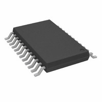
AD7739BRU Analog Devices Inc, AD7739BRU Datasheet - Page 16

AD7739BRU
Manufacturer Part Number
AD7739BRU
Description
IC ADC 24BIT 8-CH 24-TSSOP
Manufacturer
Analog Devices Inc
Datasheet
1.AD7739BRUZ.pdf
(32 pages)
Specifications of AD7739BRU
Rohs Status
RoHS non-compliant
Number Of Bits
24
Sampling Rate (per Second)
15.1k
Data Interface
DSP, MICROWIRE™, QSPI™, Serial, SPI™
Number Of Converters
1
Power Dissipation (max)
100mW
Voltage Supply Source
Analog and Digital
Operating Temperature
-40°C ~ 105°C
Mounting Type
Surface Mount
Package / Case
24-TSSOP (0.173", 4.40mm Width)
For Use With
EVAL-AD7739EBZ - BOARD EVAL FOR AD7739
Available stocks
Company
Part Number
Manufacturer
Quantity
Price
Company:
Part Number:
AD7739BRUZ
Manufacturer:
ADI
Quantity:
1 000
Company:
Part Number:
AD7739BRUZ
Manufacturer:
Analog Devices Inc
Quantity:
1 859
Part Number:
AD7739BRUZ
Manufacturer:
ADI/亚德诺
Quantity:
20 000
Company:
Part Number:
AD7739BRUZ-REEL7
Manufacturer:
ADI
Quantity:
1 000
AD7739
I/O PORT REGISTER
8 Bits, Read/Write Register, Address 0x01, Default Value 0x30 + Digital Input Value × 0x40
The bits in this register are used to configure and access the digital I/O port on the AD7739.
Bit
Mnemonic
Default
Bit
7, 6
5, 4
3
2
1
0
REVISION REGISTER
8 Bits, Read-Only Register, Address 0x02, Default Value 0x09 + Chip Revision × 0x10
Bit
Mnemonic
Default
Bit
7–4
3–0
TEST REGISTER
24 Bits, Read/Write Register, Address 0x03
This register is used for testing the part in the manufacturing process. The user must not change the default configuration of this register.
Mnemonic
P0, P1
P0 DIR, P1 DIR
RDYFN
REDPWR
0
SYNC
Mnemonic
Chip Revision Code
Chip Generic Code
Bit 7
P0
P0 Pin
Description
When the P0 and P1 pins are configured as outputs, the P0 and P1 bits determine the pins’ output level. When
the P0 and P1 pins are configured as inputs, the P0 and P1 bits reflect the current input level on the pins.
These bits determine whether the P0 and P1 pins are configured as inputs or outputs. When set to 1, the
corresponding pin will be an input; when reset to 0, the corresponding pin will be an output.
This bit is used to control the function of the RDY pin on the AD7739. When this bit is reset to 0, the RDY pin
goes low when any channel has unread data. When this bit is set to 1, the RDY pin will go low only if all
enabled channels have unread data.
Reduced Power. If this bit is set to 1, the AD7739 works in the reduced power mode. The maximum MCLK
frequency is limited to 4 MHz in the reduced power mode.
This bit must be 0 for proper operation.
This bit enables the SYNC pin function. By default, this bit is 0 and SYNC/P1 can be used as a digital I/O pin.
When the SYNC bit is set to 1, the SYNC pin can be used to synchronize the AD7739 modulator and digital
filter with other devices in the system.
Bit 7
x
Description
4-Bit Factory Chip Revision Code
On the AD7739, these bits will read back as 0x09.
Bit 6
P1 Pin
Bit 6
x
P1
Chip Revision Code
Bit 5
x
Bit 5
P0 DIR
1
Rev. 0 | Page 16 of 32
Bit 4
x
Bit 4
P1 DIR
1
Bit 3
RDYFN
0
Bit 3
1
Bit 2
REDPWR
0
Bit 2
0
Chip Generic Code
Bit 1
0
0
Bit 1
0
Bit 0
Bit 0
1
SYNC
0


