AD7715ANZ-3 Analog Devices Inc, AD7715ANZ-3 Datasheet - Page 5
AD7715ANZ-3
Manufacturer Part Number
AD7715ANZ-3
Description
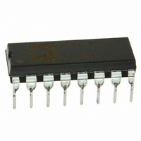
IC ADC 16BIT SIGMA-DELTA 16DIP
Manufacturer
Analog Devices Inc
Specifications of AD7715ANZ-3
Data Interface
DSP, MICROWIRE™, QSPI™, Serial, SPI™
Number Of Bits
16
Sampling Rate (per Second)
500
Number Of Converters
1
Power Dissipation (max)
9.5mW
Voltage Supply Source
Analog and Digital
Operating Temperature
-40°C ~ 85°C
Mounting Type
Through Hole
Package / Case
16-DIP (0.300", 7.62mm)
Resolution (bits)
16bit
Input Channel Type
Differential
Supply Voltage Range - Analogue
3V To 3.6V
Supply Voltage Range - Digital
3V To 5.25V
Supply Current
600µA
No. Of
RoHS Compliant
Sampling Rate
19.2kSPS
Rohs Compliant
Yes
Lead Free Status / RoHS Status
Lead free / RoHS Compliant
For Use With
EVAL-AD7715-3EBZ - BOARD EVALUATION FOR AD7715
Lead Free Status / RoHS Status
Lead free / RoHS Compliant
Available stocks
Company
Part Number
Manufacturer
Quantity
Price
Company:

Part Number:
AD7715ANZ-3
Manufacturer:
INFINEON
Quantity:
12
Part Number:
AD7715ANZ-3
Manufacturer:
ADI/亚德诺
Quantity:
20 000


REV. C
Parameter
f
t
t
t
t
Read Operation
Write Operation
NOTES
1
2
3
4
5
6
7
Specifications subject to change without notice.
TIMING CHARACTERISTICS
CLKIN
Sample tested at +25 C to ensure compliance. All input signals are specified with tr = tf = 5 ns (10% to 90% of D V
See Figures 6 and 7.
CLKIN Duty Cycle range is 45% to 55%. CLKIN must be supplied whenever the AD7715 is not in Standby mode. If no clock is present in this case, the
The AD7715 is production tested with f
These numbers are measured with the load circuit of Figure 1 and defined as the time required for the output to cross the V
These numbers are derived from the measured time taken by the data output to change 0.5 V when loaded with the circuit of Figure 1. The measured number is
DRDY returns high after the first read from the device after an output update. The same data can be read again, if required, while DRDY is high although care
CLK IN LO
CLK IN HI
1
2
device can draw higher current than specified and possibly become uncalibrated.
then extrapolated back to remove effects of charging or discharging the 50 pF capacitor. This means that the times quoted in the timing characteristics are the
true bus relinquish times of the part and as such are independent of external bus loading capacitances.
should be taken that subsequent reads do not occur close to the next output update.
t
t
t
t
t
t
t
t
t
t
t
t
t
t
3
4
5
6
7
8
9
10
11
12
13
14
15
16
5
6
3, 4
Limit at T
(A Version)
400
2.5
0.4
0.4
500
100
0
120
0
80
100
100
100
0
10
60
100
100
120
30
20
100
100
0
t
t
t
CLK IN
CLK IN
Figure 1. Load Circuit for Access Time and Bus Relinquish Time
CLK IN
CLKIN
MIN
, T
at 2.4576 MHz (1 MHz for some I
MAX
1, 2
OUTPUT
PIN
(DV
Input Logic 0 = 0 V, Logic 1 = DV
TO
DD
Unit
kHz min
MHz max
ns min
ns min
ns nom
ns min
ns min
ns min
ns min
ns max
ns max
ns min
ns min
ns min
ns min
ns max
ns max
ns max
ns min
ns min
ns min
ns min
ns min
ns min
50pF
= +3 V to +5.25 V; AV
I
I
SINK
SOURCE
Conditions/Comments
Master Clock Frequency: Crystal Oscillator or Externally Supplied
for Specified Performance
Master Clock Input Low Time. t
Master Clock Input High Time
DRDY High Time
RESET Pulsewidth
DRDY to CS Setup Time
CS Falling Edge to SCLK Rising Edge Setup Time
SCLK Falling Edge to Data Valid Delay
DV
DV
SCLK High Pulsewidth
SCLK Low Pulsewidth
CS Rising Edge to SCLK Rising Edge Hold Time
Bus Relinquish Time after SCLK Rising Edge
DV
DV
SCLK Falling Edge to DRDY High
CS Falling Edge to SCLK Rising Edge Setup Time
Data Valid to SCLK Rising Edge Setup Time
Data Valid to SCLK Rising Edge Hold Time
SCLK High Pulsewidth
SCLK Low Pulsewidth
CS Rising Edge to SCLK Rising Edge Hold Time
–5–
DD
(800 A AT DV
DD
DD
DD
DD
100 A AT DV
tests). It is guaranteed by characterization to operate at 400 kHz.
(200 A AT DV
100 A AT DV
= +5 V
= +3.3 V
= +5 V
= +3.3 V
DD
+1.6V
= +3 V to +5.25 V; AGND = DGND = 0 V; f
DD
DD
DD
, unless otherwise noted)
= 3.3V)
= 5V
DD
DD
= 5V
= 3.3V)
DD
) and timed from a voltage level of 1.6 V.
CLK IN
7
OL
= 1/f
or V
OH
CLK IN
limits.
CLKIN
= 2.4576 MHz;
AD7715
Related parts for AD7715ANZ-3
Image
Part Number
Description
Manufacturer
Datasheet
Request
R

Part Number:
Description:
±1.7g Dual-Axis IMEMS Accelerometer Evaluation Board
Manufacturer:
Analog Devices Inc
Datasheet:

Part Number:
Description:
Inertial Sensor Evaluation System
Manufacturer:
Analog Devices Inc
Datasheet:
Part Number:
Description:
Manufacturer:
Analog Devices Inc
Datasheet:
Part Number:
Description:
Manufacturer:
Analog Devices Inc
Datasheet:
Part Number:
Description:
Manufacturer:
Analog Devices Inc
Datasheet:
Part Number:
Description:
Manufacturer:
Analog Devices Inc
Datasheet:
Part Number:
Description:
Manufacturer:
Analog Devices Inc
Datasheet:
Part Number:
Description:
Manufacturer:
Analog Devices Inc
Datasheet:
Part Number:
Description:
Manufacturer:
Analog Devices Inc
Datasheet:
Part Number:
Description:
Manufacturer:
Analog Devices Inc
Datasheet:
Part Number:
Description:
Manufacturer:
Analog Devices Inc
Datasheet:
Part Number:
Description:
Manufacturer:
Analog Devices Inc
Datasheet:
Part Number:
Description:
Manufacturer:
Analog Devices Inc
Datasheet: