AD7715ANZ-3 Analog Devices Inc, AD7715ANZ-3 Datasheet - Page 2
AD7715ANZ-3
Manufacturer Part Number
AD7715ANZ-3
Description
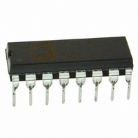
IC ADC 16BIT SIGMA-DELTA 16DIP
Manufacturer
Analog Devices Inc
Specifications of AD7715ANZ-3
Data Interface
DSP, MICROWIRE™, QSPI™, Serial, SPI™
Number Of Bits
16
Sampling Rate (per Second)
500
Number Of Converters
1
Power Dissipation (max)
9.5mW
Voltage Supply Source
Analog and Digital
Operating Temperature
-40°C ~ 85°C
Mounting Type
Through Hole
Package / Case
16-DIP (0.300", 7.62mm)
Resolution (bits)
16bit
Input Channel Type
Differential
Supply Voltage Range - Analogue
3V To 3.6V
Supply Voltage Range - Digital
3V To 5.25V
Supply Current
600µA
No. Of
RoHS Compliant
Sampling Rate
19.2kSPS
Rohs Compliant
Yes
Lead Free Status / RoHS Status
Lead free / RoHS Compliant
For Use With
EVAL-AD7715-3EBZ - BOARD EVALUATION FOR AD7715
Lead Free Status / RoHS Status
Lead free / RoHS Compliant
Available stocks
Company
Part Number
Manufacturer
Quantity
Price
Company:

Part Number:
AD7715ANZ-3
Manufacturer:
INFINEON
Quantity:
12
Part Number:
AD7715ANZ-3
Manufacturer:
ADI/亚德诺
Quantity:
20 000


f
AD7715-5–SPECIFICATIONS
Parameter
STATIC PERFORMANCE
ANALOG INPUTS/REFERENCE INPUTS
LOGIC INPUTS
LOGIC OUTPUTS (Including MCLK OUT)
CLK IN
No Missing Codes
Output Noise
Integral Nonlinearity
Unipolar Offset Error
Unipolar Offset Drift
Bipolar Zero Error
Bipolar Zero Drift
Positive Full-Scale Error
Full-Scale Drift
Gain Error
Gain Drift
Bipolar Negative Full-Scale Error
Bipolar Negative Full-Scale Drift
Input Common-Mode Rejection (CMR)
Normal-Mode 50 Hz Rejection
Normal-Mode 60 Hz Rejection
Common-Mode 50 Hz Rejection
Common-Mode 60 Hz Rejection
Common-Mode Voltage Range
Absolute AIN/REF IN Voltage
Absolute/Common-Mode AIN Voltage
AIN DC Input Current
AIN Sampling Capacitance
AIN Differential Voltage Range
AIN Input Sampling Rate, f
REF IN(+) – REF IN(–) Voltage
REF IN Input Sampling Rate, f
Input Current
All Inputs Except MCLK IN
MCLK IN Only
V
V
V
V
Floating State Leakage Current
Floating State Output Capacitance
Data Output Coding
OL
OL
OH
OH
= 2.4576 MHz unless otherwise noted. All specifications T
V
V
V
V
V
V
V
V
, Output Low Voltage
, Output Low Voltage
INL
INL
INH
INH
INL
INL
INH
INH
, Output High Voltage
, Output High Voltage
, Input Low Voltage
, Input Low Voltage
, Input Low Voltage
, Input Low Voltage
, Input High Voltage
, Input High Voltage
, Input High Voltage
, Input High Voltage
3, 7
6
3, 5
3
3
8
4
8
S
8
8
8
9
10
S
3
8
8
2
13
9
A Version
16
See Tables V to VIII
See Note 2
0.5
See Note 2
0.5
See Note 2
0.5
See Note 2
0.5
1
0.6
90
98
98
150
150
AGND to AV
AGND – 30 mV
AV
AGND + 50 mV
AV
1
10
0 to +V
GAIN
f
+2.5
f
0.8
0.4
2.4
2.0
0.8
0.4
3.5
2.5
0.4
0.4
4.0
DV
9
Binary
Offset Binary
CLK IN
CLK IN
0.0015
0.0015
V
10
10
DD
DD
REF
DD
/GAIN
+ 30 mV
– 1.5 V
/8
/64
– 0.6 V
REF
f
CLK IN
/GAIN
1
DD
/64
(AV
11
MIN
DD
= +5 V, DV
to T
Unit
Bits min
% of FSR max
ppm of FSR/ C typ
% of FSR max
dB min
dB min
dB min
dB min
dB min
V min to V max
V min
V max
V min
V max
nA max
pF max
nom
nom
V nom
V max
V max
V min
V min
V max
V max
V min
V min
V max
V max
V min
V min
pF typ
V/ C typ
V/ C typ
V/ C typ
V/ C typ
V/ C typ
A max
A max
–2–
MAX
unless otherwise noted.)
DD
= +3 V or +5 V, REF IN(+) = +2.5 V; REF IN(–) = AGND;
Conditions/Comments
Guaranteed by Design. Filter Notch
Depends on Filter Cutoffs and Selected Gain
Filter Notch
Typically 0.0004%
For Gains of 1 and 2
For Gains of 32 and 128
Specifications for AIN and REF IN Unless Noted
at DC. Typically 102 dB
For Filter Notches of 25 Hz, 50 Hz, 0.02
For Filter Notches of 20 Hz, 60 Hz, 0.02
For Filter Notches of 25 Hz, 50 Hz, 0.02
For Filter Notches of 20 Hz, 60 Hz, 0.02
AIN for BUF Bit of Setup Register = 0 and REF IN
AIN for BUF Bit of Setup Register = 0 and REF IN
BUF Bit of Setup Register = 1
Unipolar Input Range (B/U Bit of Setup Register = 1)
Bipolar Input Range (B/U Bit of Setup Register = 0)
For Gains of 1 and 2
For Gains of 32 and 128
Lower V
DV
DV
DV
DV
DV
DV
DV
I
I
I
I
Unipolar Mode
Bipolar Mode
SINK
SINK
SOURCE
SOURCE
1% for Specified Performance. Functional with
DD
DD
DD
DD
DD
DD
DD
= 100 A Except for MCLK OUT
= 800 A Except for MCLK OUT
= +5 V
= +3.3 V
= +5 V
= +5 V
= +3.3 V
= +5 V
= +3.3 V
= 200 A Except for MCLK OUT
= 100 A Except for MCLK OUT
REF
60 Hz
12
12
60 Hz
. DV
. DV
12
12
. DV
. DV
DD
DD
f
f
f
f
NOTCH
NOTCH
NOTCH
NOTCH
DD
DD
= +5 V
= +3.3 V
REV. C
= +5 V
= +3.3 V
Related parts for AD7715ANZ-3
Image
Part Number
Description
Manufacturer
Datasheet
Request
R

Part Number:
Description:
±1.7g Dual-Axis IMEMS Accelerometer Evaluation Board
Manufacturer:
Analog Devices Inc
Datasheet:

Part Number:
Description:
Inertial Sensor Evaluation System
Manufacturer:
Analog Devices Inc
Datasheet:
Part Number:
Description:
Manufacturer:
Analog Devices Inc
Datasheet:
Part Number:
Description:
Manufacturer:
Analog Devices Inc
Datasheet:
Part Number:
Description:
Manufacturer:
Analog Devices Inc
Datasheet:
Part Number:
Description:
Manufacturer:
Analog Devices Inc
Datasheet:
Part Number:
Description:
Manufacturer:
Analog Devices Inc
Datasheet:
Part Number:
Description:
Manufacturer:
Analog Devices Inc
Datasheet:
Part Number:
Description:
Manufacturer:
Analog Devices Inc
Datasheet:
Part Number:
Description:
Manufacturer:
Analog Devices Inc
Datasheet:
Part Number:
Description:
Manufacturer:
Analog Devices Inc
Datasheet:
Part Number:
Description:
Manufacturer:
Analog Devices Inc
Datasheet:
Part Number:
Description:
Manufacturer:
Analog Devices Inc
Datasheet: