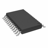
AD7366BRUZ-5 Analog Devices Inc, AD7366BRUZ-5 Datasheet - Page 26

AD7366BRUZ-5
Manufacturer Part Number
AD7366BRUZ-5
Description
IC ADC 12BIT DUAL 500KSPS 24-TSS
Manufacturer
Analog Devices Inc
Datasheet
1.AD7367BRUZ-5.pdf
(28 pages)
Specifications of AD7366BRUZ-5
Data Interface
DSP, MICROWIRE™, QSPI™, Serial, SPI™
Design Resources
Driving the AD7366/7 Bipolar SAR ADC in Low-Distortion DC-Coupled Appls (CN0042)
Number Of Bits
12
Sampling Rate (per Second)
500k
Number Of Converters
2
Power Dissipation (max)
88.8mW
Voltage Supply Source
Analog and Digital, Dual ±
Operating Temperature
-40°C ~ 85°C
Mounting Type
Surface Mount
Package / Case
24-TSSOP (0.173", 4.40mm Width)
Resolution (bits)
12bit
Input Channel Type
Single Ended
Supply Voltage Range - Analogue
4.75V To 5.25V, ± 11.5V To ± 16.5V
Supply Voltage Range - Digital
2.7V To 5.25V,
Sampling Rate
1MSPS
Rohs Compliant
Yes
Lead Free Status / RoHS Status
Lead free / RoHS Compliant
For Use With
EVAL-AD7366CBZ - BOARD EVALUATION FOR AD7366
Lead Free Status / RoHS Status
Lead free / RoHS Compliant, Lead free / RoHS Compliant
Available stocks
Company
Part Number
Manufacturer
Quantity
Price
Company:
Part Number:
AD7366BRUZ-5
Manufacturer:
ADI
Quantity:
1 000
Part Number:
AD7366BRUZ-5
Manufacturer:
ADI/亚德诺
Quantity:
20 000
Company:
Part Number:
AD7366BRUZ-5-RL7
Manufacturer:
ADI
Quantity:
1 000
AD7366-5/AD7367-5
AD7366-5/AD7367-5 TO DSP563xx
The connection diagram in Figure 32 shows how the AD7366-5/
AD7367-5 can be connected to the enhanced synchronous
serial interface (ESSI) of the DSP563xx family of DSPs from
Motorola. There are two on-board ESSIs, and each is operated in
synchronous mode (Bit SYN = 1 in the CRB register) with
internally generated word length frame sync for both Tx and Rx
(Bit FSL1 = 0 and Bit FSL0 = 0 in the CRB register).
*ADDITIONAL PINS OMITTED FOR CLARITY.
Figure 32. Interfacing the AD7366-5/AD7367-5 to the DSP563xx
AD7367-5*
AD7366-5/
CNVST
D
D
V
SCLK
BUSY
OUT
DRIVE
OUT
CS
A
B
SCK0
SCK1
SRD0
SRD1
SC02
SC12
IRQn
PBn
DSP563xx*
V
DD
Rev. A | Page 26 of 28
Normal operation of the ESSI is selected by making MOD = 0 in
the CRB register. Set the word length to 16 by setting Bit WL1 = 1
and Bit WL0 = 0 in the CRA register. The FSP bit in the CRB
register should be set to 1 so that the frame sync is negative.
In Figure 32, the serial clock is taken from the ESSI0 so the SCK0
pin must be set as an output (SCKD = 1) while the SCK1 pin is set
as an input (SCKD = 0). The frame sync signal is taken from SC02
on ESSI0, so SCD2 = 1, while on ESSI1, SCD2 = 0; therefore, SC12
is configured as an input. The V
AD7367-5 takes the same supply voltage as that of the DSP563xx.
This allows the ADC to operate at a higher voltage than its
serial interface and, therefore, the DSP563xx, if necessary.
DRIVE
pin of the AD7366-5/


