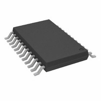
AD7366BRUZ-5 Analog Devices Inc, AD7366BRUZ-5 Datasheet - Page 25

AD7366BRUZ-5
Manufacturer Part Number
AD7366BRUZ-5
Description
IC ADC 12BIT DUAL 500KSPS 24-TSS
Manufacturer
Analog Devices Inc
Datasheet
1.AD7367BRUZ-5.pdf
(28 pages)
Specifications of AD7366BRUZ-5
Data Interface
DSP, MICROWIRE™, QSPI™, Serial, SPI™
Design Resources
Driving the AD7366/7 Bipolar SAR ADC in Low-Distortion DC-Coupled Appls (CN0042)
Number Of Bits
12
Sampling Rate (per Second)
500k
Number Of Converters
2
Power Dissipation (max)
88.8mW
Voltage Supply Source
Analog and Digital, Dual ±
Operating Temperature
-40°C ~ 85°C
Mounting Type
Surface Mount
Package / Case
24-TSSOP (0.173", 4.40mm Width)
Resolution (bits)
12bit
Input Channel Type
Single Ended
Supply Voltage Range - Analogue
4.75V To 5.25V, ± 11.5V To ± 16.5V
Supply Voltage Range - Digital
2.7V To 5.25V,
Sampling Rate
1MSPS
Rohs Compliant
Yes
Lead Free Status / RoHS Status
Lead free / RoHS Compliant
For Use With
EVAL-AD7366CBZ - BOARD EVALUATION FOR AD7366
Lead Free Status / RoHS Status
Lead free / RoHS Compliant, Lead free / RoHS Compliant
Available stocks
Company
Part Number
Manufacturer
Quantity
Price
Company:
Part Number:
AD7366BRUZ-5
Manufacturer:
ADI
Quantity:
1 000
Part Number:
AD7366BRUZ-5
Manufacturer:
ADI/亚德诺
Quantity:
20 000
Company:
Part Number:
AD7366BRUZ-5-RL7
Manufacturer:
ADI
Quantity:
1 000
AD7366-5/AD7367-5 TO ADSP-BF53x
The ADSP-BF53x family of DSPs interfaces directly to the
AD7366-5/AD7367-5 with no glue logic required. The availability
of secondary receive registers on the serial ports of the Blackfin®
DSPs means that only one serial port is necessary to read from
both D
D
Serial Port 0 of the ADSP-BF53x. The SPORT0 Receive
Configuration 1 register and SPORT0 Receive Configuration 2
register should be set up as outlined in Table 13 and Table 14.
Table 13. SPORT0 Receive Configuration 1 Register
(SPORT0_RCR1) Setup
Setting
RCKFE = 1
LRFS = 1
RFSR = 1
IRFS = 1
RLSBIT = 0
RDTYPE = 00
IRCLK = 1
RSPEN = 1
SLEN = 1111
TFSR = RFSR = 1
Table 14. SPORT0 Receive Configuration 2 Register
(SPORT0_RCR2) Setup
Setting
RXSE = 1
SLEN = 1111
OUT
*ADDITIONAL PINS OMITTED FOR CLARITY.
Figure 30. Interfacing the AD7366-5/AD7367-5 to the ADSP-BF53x
A and D
OUT
AD7367-5*
AD7366-5/
A and D
OUT
CNVST
D
V
D
BUSY
B of the AD7366-5/AD7367-5 connected to
SCLK
OUT
DRIVE
Description
Secondary side enabled.
16-bit data-word (or can be set to 1101 for
14-bit data-word).
OUT
CS
OUT
B
A
Description
Sample data with falling edge of RSCLK.
Active low frame signal.
Frame every word.
Internal RFS used.
Receive MSB first.
Zero fill.
Internal receive clock.
Receive enabled.
16-bit data-word (or can be set to 1101 for
14-bit data-word).
B pins simultaneously. Figure 30 shows
(SECONDARY)
(PRIMARY)
DEVICE A
DEVICE B
SERIAL
SERIAL
DR0PRI
RCLKO
RFS0
RXINPUTS
PFn
DR0SEC
SPORT0
ADSP-BF53x*
V
DD
Rev. A | Page 25 of 28
AD7366-5/AD7367-5 TO TMS320VC5506
The serial interface on the TMS320VC5506 uses a continuous
serial clock and frame synchronization signals to synchronize
the data transfer operations with peripheral devices like the
AD7366-5/AD7367-5. The CS input allows easy interfacing
between the TMS320VC5506 and the AD7366-5/AD7367-5
with no glue logic required. The serial ports of the TMS320VC5506
are set up to operate in burst mode with internal CLKX0 (Tx
serial clock on Serial Port 0) and FSX0 (Tx frame sync from
Serial Port 0). The connection diagram is shown in
The serial port control registers (SPC) must be setup as shown
in
Table 15. Serial Port Control Register Setup
SPC
SPC0
SPC1
The V
supply voltage as that of the TMS320VC5506. This allows the
ADC to operate at a higher voltage than its serial interface and,
therefore, the TMS320VC5506, if necessary.
As with the previous interfaces, conversion can be initiated
from the TMS320VC5506 or from an external source, and the
processor is interrupted when the conversion sequence is
complete.
Table 15
Figure 31. Interfacing the AD7366-5/AD7367-5 to the TMS320VC5506
*ADDITIONAL PINS OMITTED FOR CLARITY.
DRIVE
AD7366-5/
AD7367-5*
.
pin of the AD7366-5/AD7367-5 takes the same
FO
0
0
CNVST
D
D
V
BUSY
SCLK
OUT
OUT
DRIVE
CS
A
B
FSM
1
1
AD7366-5/AD7367-5
MCM
1
0
CLKX0
CLKR0
CLKX1
CLKR1
DR0
DR1
FSX0
FSR0
FSR1
INTn
XF
TMS320VC5506*
V
DD
Figure 31
TXM
1
0
.


