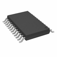
AD7366BRUZ-5 Analog Devices Inc, AD7366BRUZ-5 Datasheet - Page 24

AD7366BRUZ-5
Manufacturer Part Number
AD7366BRUZ-5
Description
IC ADC 12BIT DUAL 500KSPS 24-TSS
Manufacturer
Analog Devices Inc
Datasheet
1.AD7367BRUZ-5.pdf
(28 pages)
Specifications of AD7366BRUZ-5
Data Interface
DSP, MICROWIRE™, QSPI™, Serial, SPI™
Design Resources
Driving the AD7366/7 Bipolar SAR ADC in Low-Distortion DC-Coupled Appls (CN0042)
Number Of Bits
12
Sampling Rate (per Second)
500k
Number Of Converters
2
Power Dissipation (max)
88.8mW
Voltage Supply Source
Analog and Digital, Dual ±
Operating Temperature
-40°C ~ 85°C
Mounting Type
Surface Mount
Package / Case
24-TSSOP (0.173", 4.40mm Width)
Resolution (bits)
12bit
Input Channel Type
Single Ended
Supply Voltage Range - Analogue
4.75V To 5.25V, ± 11.5V To ± 16.5V
Supply Voltage Range - Digital
2.7V To 5.25V,
Sampling Rate
1MSPS
Rohs Compliant
Yes
Lead Free Status / RoHS Status
Lead free / RoHS Compliant
For Use With
EVAL-AD7366CBZ - BOARD EVALUATION FOR AD7366
Lead Free Status / RoHS Status
Lead free / RoHS Compliant, Lead free / RoHS Compliant
Available stocks
Company
Part Number
Manufacturer
Quantity
Price
Company:
Part Number:
AD7366BRUZ-5
Manufacturer:
ADI
Quantity:
1 000
Part Number:
AD7366BRUZ-5
Manufacturer:
ADI/亚德诺
Quantity:
20 000
Company:
Part Number:
AD7366BRUZ-5-RL7
Manufacturer:
ADI
Quantity:
1 000
AD7366-5/AD7367-5
MICROPROCESSOR INTERFACING
The serial interface on the AD7366-5/AD7367-5 allows the
parts to be directly connected to a range of different micro-
processors. This section explains how to interface the AD7366-5/
AD7367-5 with some more common microcontrollers and DSP
serial interface protocols.
AD7366-5/AD7367-5 TO ADSP-218x
The ADSP-218x family of DSPs interfaces directly to the
AD7366-5/AD7367-5 with no glue logic required. The V
pin of the AD7366-5/AD7367-5 takes the same supply voltage
as that of the ADSP-218x. This allows the ADC to operate at a
higher supply voltage than its serial interface and therefore, the
ADSP-218x, if necessary. The connection diagram in Figure 29
shows both D
connected to both serial ports of the ADSP-218x. The SPORT0
and SPORT1 control registers should be set up as shown in
Table 11 and Table 12.
*ADDITIONAL PINS OMITTED FOR CLARITY.
Figure 29. Interfacing the AD7366-5/AD7367-5 to the ADSP-218x
AD7366-5/
AD7367-5*
OUT
CNVST
D
D
V
BUSY
SCLK
OUT
OUT
DRIVE
A and D
CS
A
B
OUT
B of the AD7366-5/AD7367-5
SCLK0
SCLK1
TFS0
RFS0
RFS1
DR0
DR1
IRQn
FLn
ADSP-218x*
V
DD
DRIVE
Rev. A | Page 24 of 28
Table 11. SPORT0 Control Register Setup
Setting
TFSW = RFSW = 1
INVRFS = INVTFS = 1
DTYPE = 00
SLEN = 1111
ISCLK = 1
TFSR = RFSR = 1
IRFS = 0
ITFS = 1
Table 12. SPORT1 Control Register Setup
Setting
TFSW = RFSW = 1
INVRFS = INVTFS = 1
DTYPE = 00
SLEN = 1111
ISCLK = 0
TFSR = RFSR = 1
IRFS = 0
ITFS = 1
The ADSP-218x has the TFS0 and RFS0 of the SPORT0 and the
RFS1 of SPORT1 tied together. TFS0 is set as an output, and both
RFS0 and RFS1 are set as inputs. The DSP operates in alternate
framing mode, and the SPORT control registers are set up as
described in Table 11 and Table 12. The frame synchronization
signal generated on the TFS0 is tied to CS .
The AD7366-5/AD7367-5 BUSY line provides an interrupt to
the ADSP-218x when the conversion is complete. The conversion
results can then be read from the AD7366-5/AD7367-5 using a
read operation. When an interrupt is received on IRQn from the
BUSY signal, a value is transmitted with TFS/DT (ADC control
word). The TFS is used to control the RFS and, therefore, the
reading of data.
Description
Alternate framing.
Active low frame signal.
Right justify data.
16-bit data-word (or can be set to 1101
for 14-bit data-word).
Internal serial clock.
Frame every word.
Description
Alternate framing.
Active low frame signal.
Right justify data.
16-bit data-word (or can be set to 1101
for 14-bit data-word).
External serial clock.
Frame every word.


