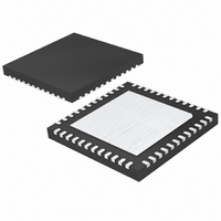
LTC2206IUK-14#PBF Linear Technology, LTC2206IUK-14#PBF Datasheet - Page 24

LTC2206IUK-14#PBF
Manufacturer Part Number
LTC2206IUK-14#PBF
Description
IC ADC 14BIT 80MSPS 48-QFN
Manufacturer
Linear Technology
Datasheet
1.LTC2206CUK-14PBF.pdf
(32 pages)
Specifications of LTC2206IUK-14#PBF
Number Of Bits
14
Sampling Rate (per Second)
80M
Data Interface
Parallel
Number Of Converters
1
Power Dissipation (max)
875mW
Voltage Supply Source
Single Supply
Operating Temperature
-40°C ~ 85°C
Mounting Type
Surface Mount
Package / Case
48-WFQFN, Exposed Pad
Lead Free Status / RoHS Status
Lead free / RoHS Compliant
Available stocks
Company
Part Number
Manufacturer
Quantity
Price
LTC2207-14/LTC2206-14
APPLICATIONS INFORMATION
converter data to the digital system. This is necessary
when using a sinusoidal encode. Data can be latched on the
rising edge of CLKOUT+ or the falling edge of CLKOUT–.
CLKOUT+ falls and CLKOUT– rises as the data outputs
are updated.
Digital Output Randomizer
Interference from the ADC digital outputs is sometimes
unavoidable. Interference from the digital outputs may be
from capacitive or inductive coupling or coupling through
the ground plane. Even a tiny coupling factor can result in
discernible unwanted tones in the ADC output spectrum.
By randomizing the digital output before it is transmitted
off chip, these unwanted tones can be randomized, trading
a slight increase in the noise fl oor for a large reduction in
unwanted tone amplitude.
The digital output is “Randomized” by applying an exclu-
sive-OR logic operation between the LSB and all other data
output bits. To decode, the reverse operation is applied;
that is, an exclusive-OR operation is applied between the
LSB and all other bits. The LSB, OF and CLKOUT outputs
are not affected. The output Randomizer function is active
when the RAND pin is high.
24
PC BOARD
LTC2207-14/
LTC2206-14
Figure 13. Descrambling a Scrambled Digital Output
CLKOUT
D13/D0
D12/D0
D2/D0
D1/D0
D0
OF
Output Driver Power
Separate output power and ground pins allow the output
drivers to be isolated from the analog circuitry. The power
supply for the digital output buffers, OV
to the same power supply as for the logic being driven.
For example, if the converter is driving a DSP powered
by a 1.8V supply, then OV
1.8V supply. In CMOS mode OV
any logic voltage up to the V
powered with any voltage from ground up to 1V and must
be less than OV
OGND and OV
Internal Dither
The LTC2207-14/LTC2206-14 are 14-bit ADCs with a very
linear transfer function; however, at low input levels even
slight imperfections in the transfer function will result in
unwanted tones. Small errors in the transfer function are
usually a result of ADC element mismatches. An optional
internal dither mode can be enabled to randomize the input
location on the ADC transfer curve, resulting in improved
SFDR for low signal levels.
FPGA
•
•
•
DD
DD
.
D13
D12
D2
D1
D0
. The logic outputs will swing between
2207614 F13
DD
DD
should be tied to that same
of the ADC. OGND can be
DD
can be powered with
DD
, should be tied
220714614fc


