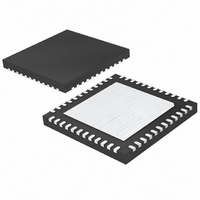
LTC2206IUK-14#PBF Linear Technology, LTC2206IUK-14#PBF Datasheet - Page 14

LTC2206IUK-14#PBF
Manufacturer Part Number
LTC2206IUK-14#PBF
Description
IC ADC 14BIT 80MSPS 48-QFN
Manufacturer
Linear Technology
Datasheet
1.LTC2206CUK-14PBF.pdf
(32 pages)
Specifications of LTC2206IUK-14#PBF
Number Of Bits
14
Sampling Rate (per Second)
80M
Data Interface
Parallel
Number Of Converters
1
Power Dissipation (max)
875mW
Voltage Supply Source
Single Supply
Operating Temperature
-40°C ~ 85°C
Mounting Type
Surface Mount
Package / Case
48-WFQFN, Exposed Pad
Lead Free Status / RoHS Status
Lead free / RoHS Compliant
Available stocks
Company
Part Number
Manufacturer
Quantity
Price
LTC2207-14/LTC2206-14
TYPICAL PERFORMANCE CHARACTERISTICS
PIN FUNCTIONS
SENSE (Pin 1): Reference Mode Select and External
Reference Input. Tie SENSE to V
2.5V bandgap reference. An external reference of 2.5V or
1.25V may be used; both reference values will set a full
scale ADC range of 2.25V (PGA = 0).
V
mon mode. Must be bypassed to ground with a minimum
of 2.2μF . Ceramic chip capacitors are recommended.
V
Bypass to GND with 0.1μF ceramic chip capacitors.
GND (Pins 5, 8, 11, 15, 48): ADC Power Ground.
A
A
ENC
sampled analog input is held on the rising edge of ENC
Internally biased to 1.6V through a 6.2k resistor. Output
data can be latched on the rising edge of ENC
ENC
sampled analog input is held on the falling edge of ENC
Internally biased to 1.6V through a 6.2k resistor. Bypass to
ground with a 0.1μF capacitor for a single-ended Encode
signal.
14
CM
DD
IN
IN
+
–
+
–
(Pin 2): 1.25V Output. Optimum voltage for input com-
(Pins 3, 4, 12, 13, 14): 3.3V Analog Supply Pin.
(Pin 6): Positive Differential Analog Input.
(Pin 7): Negative Differential Analog Input.
(Pin 10): Negative Differential Encode Input. The
(Pin 9): Positive Differential Encode Input. The
–0.2
–0.4
–0.6
–0.8
–1.0
1.0
0.8
0.6
0.4
0.2
0
0
Mid-Scale Settling After Wake
Up from Shutdown or Starting
Encode Clock
TIME AFTER WAKE-UP OR CLOCK START (μs)
50
100
150
DD
200
to select the internal
250
300 350
400
+
.
2207614 G60
450
500
+
–
.
.
SHDN (Pin 16): Power Shutdown Pin. SHDN = low results
in normal operation. SHDN = high results in powered
down analog circuitry and the digital outputs are placed
in a high impedance state.
DITH (Pin 17): Internal Dither Enable Pin. DITH = low
disables internal dither. DITH = high enables internal dither.
Refer to Internal Dither section of this data sheet for details
on dither operation.
NC (Pins 18, 19): No Connect.
D0-D13 (Pins 20-22, 26-28, 32-35 and 39-42): Digital
Outputs. D13 is the MSB.
OGND (Pins 23, 31 and 38): Output Driver Ground.
OV
Drivers. Bypass to ground with 0.1μF capacitor.
CLKOUT
at the sample rate. Latch the data on the falling edge of
CLKOUT
CLKOUT
will toggle at the sample rate. Latch the data on the rising
edge of CLKOUT
DD
(Pins 24, 25, 36, 37): Positive Supply for the Output
–1
–2
–3
–4
–5
–
–
+
5
4
3
2
1
0
.
(Pin 29): Data Valid Output. CLKOUT
0
(Pin 30): Inverted Data Valid Output. CLKOUT
Full-Scale Settling After Wake
Up from Shutdown or Starting
Encode Clock
TIME FROM WAKE-UP OR CLOCK START (μs)
100
200
+
.
300
400
500
600 700
800
2207614 G61
900
1000
–
will toggle
220714614fc
+


