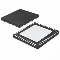
LTC2206IUK#TRPBF Linear Technology, LTC2206IUK#TRPBF Datasheet - Page 20

LTC2206IUK#TRPBF
Manufacturer Part Number
LTC2206IUK#TRPBF
Description
IC ADC 16-BIT 80MSPS 48-QFN
Manufacturer
Linear Technology
Datasheet
1.LTC2207IUKPBF.pdf
(32 pages)
Specifications of LTC2206IUK#TRPBF
Number Of Bits
16
Sampling Rate (per Second)
80M
Data Interface
Parallel
Number Of Converters
1
Power Dissipation (max)
875mW
Voltage Supply Source
Single Supply
Operating Temperature
-40°C ~ 85°C
Mounting Type
Surface Mount
Package / Case
48-WFQFN, Exposed Pad
Lead Free Status / RoHS Status
Lead free / RoHS Compliant
Available stocks
Company
Part Number
Manufacturer
Quantity
Price
LTC2207/LTC2206
APPLICATIONS INFORMATION
Direct Coupled Circuits
Figure 5 demonstrates the use of a differential amplifi er to
convert a single ended input signal into a differential input
signal. The advantage of this method is that it provides
low frequency input response; however, the limited gain
bandwidth of any op amp or closed-loop amplifi er will de-
grade the ADC SFDR at high input frequencies. Additionally,
wideband op amps or differential amplifi ers tend to have
high noise. As a result, the SNR will be degraded unless
the noise bandwidth is limited prior to the ADC input.
Reference Operation
Figure 6 shows the LTC2207/LTC2206 reference circuitry
consisting of a 2.5V bandgap reference, a programmable
gain amplifi er and control circuit. The LTC2207/LTC2206
have three modes of reference operation: Internal Refer-
ence, 1.25V external reference or 2.5V external reference.
To use the internal reference, tie the SENSE pin to V
use an external reference, simply apply either a 1.25V or
2.5V reference voltage to the SENSE input pin. Both 1.25V
and 2.5V applied to SENSE will result in a full-scale range
of 2.25V
for a common mode bias for input drive circuitry. An
external bypass capacitor is required for the V
This provides a high frequency low impedance path to
ground for internal and external circuitry. This is also the
20
ANALOG
Figure 5. DC Coupled Input with Differential Amplifi er
INPUT
P-P
AMPLIFIER = LTC6600-20,
LTC1993, ETC.
(PGA = 0). A 1.25V output V
DIFFERENTIAL
CM
–
+
HIGH SPEED
AMPLIFIER
+
–
25Ω
25Ω
2.2μF
12pF
12pF
V
A
A
CM
IN
IN
+
–
CM
LTC2207/
LTC2206
is provided
CM
22076 F05
output.
DD
. To
compensation capacitor for the reference; it will not be
stable without this capacitor. The minimum value required
for stability is 2.2μF .
The internal programmable gain amplifi er provides the
internal reference voltage for the ADC. This amplifi er has
very stringent settling requirements and is not accessible
for external use.
The SENSE pin can be driven ±5% around the nominal 2.5V
or 1.25V external reference inputs. This adjustment range
can be used to trim the ADC gain error or other system
gain errors. When selecting the internal reference, the
SENSE pin should be tied to V
as possible. If the sense pin is driven externally it should
be bypassed to ground as close to the device as possible
with 1μF (or larger) ceramic capacitor.
PGA Pin
The PGA pin selects between two gain settings for the
ADC front-end. PGA = 0 selects an input range of 2.25V
P
input range has the best SNR; however, the distortion will
be higher for input frequencies above 100MHz. For ap-
plications with high input frequencies, the low input range
will have improved distortion; however, the SNR will be
2.4dB worse. See the Typical Performance Characteristics
section of this datasheet.
TIE TO V
; PGA = 1 selects an input range of 1.5V
EXTERNAL 1.25V
EXTERNAL 2.5V
INTERNAL 2.5V
OR INPUT FOR
OR INPUT FOR
REFERENCE
REFERENCE
REFERENCE
DD
TO USE
SENSE
2.2μF
V
Figure 6. Reference Circuit
CM
LTC2207/
LTC2206
BUFFER
DD
AND GAIN
CONTROL
SELECT
RANGE
as close to the converter
1.25V
P-P
PGA
. The 2.25V
REFERENCE
BANDGAP
REFERENCE
INTERNAL
2.5V
ADC
22076fc
22076 F06
P-


