LTC2206IUK#TRPBF Linear Technology, LTC2206IUK#TRPBF Datasheet - Page 14
LTC2206IUK#TRPBF
Manufacturer Part Number
LTC2206IUK#TRPBF
Description
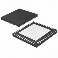
IC ADC 16-BIT 80MSPS 48-QFN
Manufacturer
Linear Technology
Datasheet
1.LTC2207IUKPBF.pdf
(32 pages)
Specifications of LTC2206IUK#TRPBF
Number Of Bits
16
Sampling Rate (per Second)
80M
Data Interface
Parallel
Number Of Converters
1
Power Dissipation (max)
875mW
Voltage Supply Source
Single Supply
Operating Temperature
-40°C ~ 85°C
Mounting Type
Surface Mount
Package / Case
48-WFQFN, Exposed Pad
Lead Free Status / RoHS Status
Lead free / RoHS Compliant
Available stocks
Company
Part Number
Manufacturer
Quantity
Price


LTC2207/LTC2206
PIN FUNCTIONS
SENSE (Pin 1): Reference Mode Select and External Refer-
ence Input. Tie SENSE to V
bandgap reference. An external reference of 2.5V or 1.25V
may be used; both reference values will set a full-scale
ADC range of 2.25V (PGA = 0).
V
mon mode. Must be bypassed to ground with a minimum
of 2.2μF . Ceramic chip capacitors are recommended.
V
Bypass to GND with 0.1μF ceramic chip capacitors.
GND (Pins 5, 8, 11, 15, 48, 49): ADC Power Ground.
A
A
ENC
sampled analog input is held on the rising edge of ENC
Internally biased to 1.6V through a 6.2kΩ resistor. Output
data can be latched on the rising edge of ENC
ENC
sampled analog input is held on the falling edge of ENC
Internally biased to 1.6V through a 6.2kΩ resistor. By-
pass to ground with a 0.1μF capacitor for a single-ended
Encode signal.
SHDN (Pin 16): Power Shutdown Pin. SHDN = low results
in normal operation. SHDN = high results in powered
down analog circuitry and the digital outputs are placed
in a high impedance state.
DITH (Pin 17): Internal Dither Enable Pin. DITH = low
disables internal dither. DITH = high enables internal dither.
Refer to Internal Dither section of this data sheet for details
on dither operation.
D0-D15 (Pins 18-22, 26-28, 32-35 and 39-42): Digital
Outputs. D15 is the MSB.
OGND (Pins 23, 31 and 38): Output Driver Ground.
14
CM
DD
IN
IN
+
–
+
–
(Pin 2): 1.25V Output. Optimum voltage for input com-
(Pins 3, 4, 12, 13, 14): 3.3V Analog Supply Pin.
(Pin 6): Positive Differential Analog Input.
(Pin 7): Negative Differential Analog Input.
(Pin 10): Negative Differential Encode Input. The
(Pin 9): Positive Differential Encode Input. The
DD
to select the internal 2.5V
+
.
+
–
.
.
OV
Drivers. Bypass to ground with 0.1μF capacitor.
CLKOUT
at the sample rate. Latch the data on the falling edge of
CLKOUT
CLKOUT
will toggle at the sample rate. Latch the data on the rising
edge of CLKOUT
OF (Pin 43): Over/Under Flow Digital Output. OF is high
when an over or under fl ow has occurred.
OE (Pin 44): Output Enable Pin. Low enables the digital
output drivers. High puts digital outputs in Hi-Z state.
MODE (Pin 45): Output Format and Clock Duty Cycle
Stabilizer Selection Pin. Connecting MODE to 0V selects
offset binary output format and disables the clock duty
cycle stabilizer. Connecting MODE to 1/3V
binary output format and enables the clock duty cycle sta-
bilizer. Connecting MODE to 2/3V
output format and enables the clock duty cycle stabilizer.
Connecting MODE to V
format and disables the clock duty cycle stabilizer.
RAND (Pin 46): Digital Output Randomization Selection
Pin. RAND low results in normal operation. RAND high
selects D1-D15 to be EXCLUSIVE-ORed with D0 (the
LSB). The output can be decoded by again applying an
XOR operation between the LSB and all other bits. This
mode of operation reduces the effects of digital output
interference.
PGA (Pin 47): Programmable Gain Amplifi er Control Pin. Low
selects a front-end gain of 1, input range of 2.25V
selects a front-end gain of 1.5, input range of 1.5V
GND (Exposed Pad, Pin 49): ADC Power Ground. The ex-
posed pad on the bottom of the package must be soldered
to ground.
DD
(Pins 24, 25, 36, 37): Positive Supply for the Output
–
–
+
.
(Pin 29): Data Valid Output. CLKOUT
(Pin 30): Inverted Data Valid Output. CLKOUT
+
.
DD
selects 2’s complement output
DD
selects 2’s complement
DD
selects offset
–
will toggle
P-P
P-P
. High
.
22076fc
+
Related parts for LTC2206IUK#TRPBF
Image
Part Number
Description
Manufacturer
Datasheet
Request
R

Part Number:
Description:
IC ADC 14-BIT 80MSPS 48-QFN
Manufacturer:
Linear Technology
Datasheet:
Part Number:
Description:
IC ADC 14BIT 80MSPS 48-QFN
Manufacturer:
Linear Technology
Datasheet:
Part Number:
Description:
IC ADC 16-BIT 80MSPS 48-QFN
Manufacturer:
Linear Technology
Datasheet:

Part Number:
Description:
IC,A/D CONVERTER,SINGLE,16-BIT,CMOS,LLCC,48PIN
Manufacturer:
Linear Technology
Part Number:
Description:
IC,A/D CONVERTER,SINGLE,16-BIT,CMOS,LLCC,48PIN
Manufacturer:
Linear Technology
Part Number:
Description:
IC,A/D CONVERTER,SINGLE,14-BIT,CMOS,LLCC,48PIN
Manufacturer:
Linear Technology
Part Number:
Description:
IC,A/D CONVERTER,SINGLE,14-BIT,CMOS,LLCC,48PIN
Manufacturer:
Linear Technology
Part Number:
Description:
CD ROM LINEARVIEW DATASHEETS
Manufacturer:
Linear Technology

Part Number:
Description:
Standalone Linear Li-Ion Battery Charger with Thermal Regulation in ThinSOT
Manufacturer:
Linear Technology Corporation
Datasheet:
Part Number:
Description:
Low noise, high frequency, 8th order linear phase lowpass filter
Manufacturer:
Linear Technology Corporation
Datasheet:
Part Number:
Description:
Manufacturer:
Linear Technology Corporation
Datasheet:
Part Number:
Description:
Manufacturer:
Linear Technology Corporation
Datasheet:
Part Number:
Description:
Manufacturer:
Linear Technology Corporation
Datasheet:
Part Number:
Description:
Manufacturer:
Linear Technology Corporation
Datasheet:
Part Number:
Description:
Manufacturer:
Linear Technology Corporation
Datasheet: