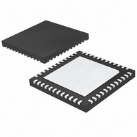
LTC2206IUK#TRPBF Linear Technology, LTC2206IUK#TRPBF Datasheet - Page 18

LTC2206IUK#TRPBF
Manufacturer Part Number
LTC2206IUK#TRPBF
Description
IC ADC 16-BIT 80MSPS 48-QFN
Manufacturer
Linear Technology
Datasheet
1.LTC2207IUKPBF.pdf
(32 pages)
Specifications of LTC2206IUK#TRPBF
Number Of Bits
16
Sampling Rate (per Second)
80M
Data Interface
Parallel
Number Of Converters
1
Power Dissipation (max)
875mW
Voltage Supply Source
Single Supply
Operating Temperature
-40°C ~ 85°C
Mounting Type
Surface Mount
Package / Case
48-WFQFN, Exposed Pad
Lead Free Status / RoHS Status
Lead free / RoHS Compliant
Available stocks
Company
Part Number
Manufacturer
Quantity
Price
LTC2207/LTC2206
APPLICATIONS INFORMATION
SAMPLE/HOLD OPERATION AND INPUT DRIVE
Sample/Hold Operation
Figure 2 shows an equivalent circuit for the LTC2207/
LTC2206 CMOS differential sample and hold. The differ-
ential analog inputs are sampled directly onto sampling
capacitors (C
capacitors shown attached to each input (C
the summation of all other capacitance associated with
each input.
During the sample phase when ENC is low, the NMOS
transistors connect the analog inputs to the sampling
capacitors and they charge to, and track the differential
input voltage. When ENC transitions from low to high, the
sampled input voltage is held on the sampling capacitors.
During the hold phase when ENC is high, the sampling
capacitors are disconnected from the input and the held
voltage is passed to the ADC core for processing. As ENC
transitions for high to low, the inputs are reconnected to
the sampling capacitors to acquire a new sample. Since
the sampling capacitors still hold the previous sample,
a charging glitch proportional to the change in voltage
between samples will be seen at this time. If the change
between the last sample and the new sample is small,
the charging glitch seen at the input will be small. If the
input change is large, such as the change seen with input
frequencies near Nyquist, then a larger charging glitch
will be seen.
Common Mode Bias
The ADC sample-and-hold circuit requires differential
drive to achieve specifi ed performance. Each input should
swing ±0.5625V for the 2.25V range (PGA = 0) or ±0.375V
for the 1.5V range (PGA = 1), around a common mode
voltage of 1.25V. The V
to provide the common mode bias level. V
directly to the center tap of a transformer to set the DC
input level or as a reference level to an op amp differential
driver circuit. The V
close to the ADC with 2.2μF or greater.
18
SAMPLE
CM
) through NMOS transistors. The
CM
pin must be bypassed to ground
output pin (Pin 2) is designed
CM
PARASITIC
can be tied
) are
Input Drive Impedence
As with all high performance, high speed ADCs the
dynamic performance of the LTC2207/LTC2206 can be
infl uenced by the input drive circuitry, particularly the
second and third harmonics. Source impedance and in-
put reactance can infl uence SFDR. At the falling edge of
ENC the sample-and-hold circuit will connect the 4.9pF
sampling capacitor to the input pin and start the sampling
period. The sampling period ends when ENC rises, hold-
ing the sampled input on the sampling capacitor. Ideally,
the input circuitry should be fast enough to fully charge
the sampling capacitor during the sampling period
1/(2F
incomplete settling may degrade the SFDR. The sampling
glitch has been designed to be as linear as possible to
minimize the effects of incomplete settling.
For the best performance it is recommended to have a
source impedence of 100Ω or less for each input. The
source impedence should be matched for the differential
inputs. Poor matching will result in higher even order
harmonics, especially the second.
ENC
ENC
A
A
IN
IN
+
+
–
–
ENCODE
LTC2207/LTC2206
1.6V
1.6V
V
); however, this is not always possible and the
DD
6k
6k
Figure 2. Equivalent Input Circuit
V
DD
V
DD
C
1.8pF
C
1.8pF
PARASITIC
PARASITIC
C
C
SAMPLE
SAMPLE
4.9pF
4.9pF
22076 F02
22076fc


