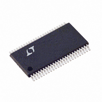
LTC1750IFW Linear Technology, LTC1750IFW Datasheet - Page 16

LTC1750IFW
Manufacturer Part Number
LTC1750IFW
Description
IC ADC 14BIT 80MSPS SMPL 48TSSOP
Manufacturer
Linear Technology
Datasheet
1.LTC1750CFW.pdf
(20 pages)
Specifications of LTC1750IFW
Number Of Bits
14
Sampling Rate (per Second)
80M
Data Interface
Parallel
Number Of Converters
1
Power Dissipation (max)
1.69W
Voltage Supply Source
Single Supply
Operating Temperature
-40°C ~ 85°C
Mounting Type
Surface Mount
Package / Case
48-TFSOP (0.240", 6.10mm Width)
Lead Free Status / RoHS Status
Contains lead / RoHS non-compliant
Available stocks
Company
Part Number
Manufacturer
Quantity
Price
Part Number:
LTC1750IFW#PBF
Manufacturer:
LINEAR/凌特
Quantity:
20 000
APPLICATIO S I FOR ATIO
LTC1750
Maximum and Minimum Encode Rates
The maximum encode rate for the LTC1750 is 80Msps. For
the ADC to operate properly the encode signal should have
a 50% ( 4%) duty cycle. Each half cycle must have at least
6ns for the ADC internal circuitry to have sufficient settling
time for proper operation. Achieving a precise 50% duty
cycle is easy with differential sinusoidal drive using a
transformer or using symmetric differential logic such as
PECL or LVDS. When using a single-ended encode signal
asymmetric rise and fall times can result in duty cycles that
are far from 50%.
At sample rates slower than 80Msps the duty cycle can
vary from 50% as long as each half cycle is at least 6ns.
The lower limit of the LTC1750 sample rate is determined
by droop of the sample-and-hold circuits. The pipelined
architecture of this ADC relies on storing analog signals on
16
V
THRESHOLD
Figure 8a. Single-Ended ENC Drive,
Not Recommended for Low Jitter
CLOCK
INPUT
U
= 2V
0.1 F
0.1 F
U
ANALOG INPUT
50
2V
ENC
ENC
W
1:4
LTC1750
1750 F08a
Figure 7. Transformer Driven ENC/ENC
ENC
ENC
U
LTC1750
V
V
DD
DD
2V BIAS
2V BIAS
6k
6k
small valued capacitors. Junction leakage will discharge
the capacitors. The specified minimum operating fre-
quency for the LTC1750 is 1Msps.
DIGITAL OUTPUTS
Digital Output Buffers
Figure 9 shows an equivalent circuit for a single output
buffer. Each buffer is powered by OV
lated from the ADC power and ground. The additional
N-channel transistor in the output driver allows operation
down to low voltages. The internal resistor in series with
the output makes the output appear as 50 to external
circuitry and may eliminate the need for external damping
resistors.
5V
Figure 8b. ENC Drive Using a CMOS-to-PECL Translator
MC100LVELT22
BIAS
D0
3.3V
Q0
Q0
130
TO INTERNAL
ADC CIRCUITS
83
3.3V
130
83
1750 F07
ENC
ENC
DD
and OGND, iso-
LTC1750
1750 F08b
1750f


