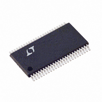
LTC1750IFW Linear Technology, LTC1750IFW Datasheet - Page 14

LTC1750IFW
Manufacturer Part Number
LTC1750IFW
Description
IC ADC 14BIT 80MSPS SMPL 48TSSOP
Manufacturer
Linear Technology
Datasheet
1.LTC1750CFW.pdf
(20 pages)
Specifications of LTC1750IFW
Number Of Bits
14
Sampling Rate (per Second)
80M
Data Interface
Parallel
Number Of Converters
1
Power Dissipation (max)
1.69W
Voltage Supply Source
Single Supply
Operating Temperature
-40°C ~ 85°C
Mounting Type
Surface Mount
Package / Case
48-TFSOP (0.240", 6.10mm Width)
Lead Free Status / RoHS Status
Contains lead / RoHS non-compliant
Available stocks
Company
Part Number
Manufacturer
Quantity
Price
Part Number:
LTC1750IFW#PBF
Manufacturer:
LINEAR/凌特
Quantity:
20 000
APPLICATIO S I FOR ATIO
LTC1750
signal conversion. Note that the two op amps do not have
the same noise gain, which can result in poor balance at
higher frequencies. The op amp configured in a gain of +1
can be configured in a noise gain of +2 with the addition of
two equal valued resistors between the output and invert-
ing input and between the two inputs. This however will raise
the noise contributed by the op amps.
Reference Operation
Figure 5 shows the LTC1750 equivalent reference circuitry
consisting of a 2V bandgap reference, a 3-to-1 switch, a
switch control circuit and a difference amplifier.
The 2V bandgap reference serves two functions. First, it is
assessable at the V
setting the common mode voltage of any external input
circuitry. Second, it is used to derive internal reference
levels that may be used to set the input range of the ADC.
An external bypass capacitor is required for the 2V refer-
ence output at the V
low impedance path to ground for internal and external
circuitry. This is also the compensation capacitor for the
reference, which will not be stable without this capacitor.
To achieve the optimal input range for an application, the
internal reference voltage (V
switch shown in Figure 5 connects V
internally derived reference voltages, or to an externally
derived reference voltage. The internally derived
14
SINGLE-ENDED
2V 1/2
RANGE
INPUT
Figure 4. Differential Drive with Op Amps
100
500
U
CM
CM
+
–
+
–
1/2 LT1818
1/2 LT1818
pin. This provides a high frequency
pin to provide a DC bias point for
5V
U
500
REF
) is flexible. The reference
25
25
W
REF
12pF
25
25
12pF
4.7 F
12pF
to one of two
U
V
A
A
CM
IN
LTC1750
IN
+
–
1750 F04
references are selected by strapping the SENSE pin to
GND for 0.7V, or to V
> 1.125V, V
of the dual nature of the SENSE pin, driving it with a logic
device is not recommended.
Reference voltages between 0.7V and 1.125V may be
programmed with two external resistors as shown in
Figure 6a. An external reference may be used by applying
its output directly or through a resistor divider to the
SENSE pin (Figure 6b). When the SENSE pin is driven with
an externally derived reference voltage, it should be by-
passed to ground as close to the device as possible with
a 1 F ceramic capacitor.
A difference amplifier generates the high and low refer-
ences for the ADC. High speed switching circuits are
connected to these outputs and they must be externally
bypassed. Each output has two pins: REFHA and REFHB
for the high reference and REFLA and REFLB for the low
reference. The doubled output pins are needed to reduce
package inductance. Bypass capacitors must be con-
nected as shown in Figure 5.
TIE TO V
TIE TO GND FOR V
0.7V < V
DD
V
FOR V
REF
SENSE
= V
REF
REF
SENSE
SENSE
Figure 5. Equivalent Reference Circuit
< 1.125V
= 1.125;
= 0.7V;
1 F
1 F
2V
FOR
is directly connected to V
4.7 F
DD
0.1 F
4.7 F
0.1 F
SENSE
REFHA
REFHB
REFLB
REFLA
for 1.125V. When 0.7V > V
V
CM
LTC1750
CONTROL
4
DETECT
RANGE
AND
DIFF AMP
2V BANDGAP
REFERENCE
INTERNAL ADC
HIGH REFERENCE
INTERNAL ADC
LOW REFERENCE
1.125V 0.7V
REF
BUFFER
. Because
SENSE
V
REF
1750f
1750 F05


