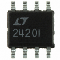
LTC2420IS8#PBF Linear Technology, LTC2420IS8#PBF Datasheet - Page 26

LTC2420IS8#PBF
Manufacturer Part Number
LTC2420IS8#PBF
Description
IC ADC 20BIT MICRPWR W/OSC 8SOIC
Manufacturer
Linear Technology
Datasheet
1.LTC2420CS8.pdf
(36 pages)
Specifications of LTC2420IS8#PBF
Number Of Bits
20
Sampling Rate (per Second)
7.5
Data Interface
MICROWIRE™, Serial, SPI™
Number Of Converters
2
Power Dissipation (max)
1mW
Voltage Supply Source
Single Supply
Operating Temperature
-40°C ~ 85°C
Mounting Type
Surface Mount
Package / Case
8-SOIC (0.154", 3.90mm Width)
Lead Free Status / RoHS Status
Lead free / RoHS Compliant
Available stocks
Company
Part Number
Manufacturer
Quantity
Price
APPLICATIO S I FOR ATIO
LTC2420
As a result of the oversampling ratio (256) and the digital
filter, minimal (if any) antialias filtering is required in front
of the LTC2420. If passive RC components are placed in
front of the LTC2420 the input dynamic current should be
considered (see Input Current section). In cases where
large effective RC time constants are used, an external
buffer amplifier may be required to minimize the effects of
input dynamic current.
The modulator contained within the LTC2420 can handle
large-signal level perturbations without saturating. Signal
levels up to 40% of V
lator. These signals are limited by the input ESD protection
to 300mV below ground and 300mV above V
Operation at Higher Data Output Rates
The LTC2420 typically operates with an internal oscillator
of 153.6kHz. This corresponds to a notch frequency of
60Hz and an output rate of 7.5 samples/second. The
internal oscillator is enabled if the F
(logic HIGH for a 50Hz notch). It is possible to drive the F
pin with an external oscillator for higher data output rates.
As shown in Figure 28, an external clock of 2.048MHz
applied to the F
with a data output rate of 100 samples/second.
Figure 29 shows the total unadjusted error (Offset Error +
Full-Scale Error + INL + DNL) as a function of the output
data rate with a 5V reference. The relationship between the
26
–100
–140
–120
–20
–40
–60
–80
0
0
Figure 27. Sinc
O
pin results in a notch frequency of 800Hz
U
REF
INPUT FREQUENCY
do not saturate the analog modu-
U
f
4
S
/2
Filter Rejection
W
O
2420 F27
pin is logic LOW
f
S
CC
U
.
O
output data rate (ODR) and the frequency applied to the F
pin (F
For output data rates up to 50 samples/second, the total
unadjusted error (TUE) is better than 16 bits, and better
than 12 bits at 100 samples/second. As shown in Figure
30, for output data rates of 100 samples/second, the TUE
is better than 15 bits for V
an unaveraged total unadjusted error for the LTC2420 op-
erating at 100 samples/second with V
shows the same device operating with a 5V reference and
an output data rate of 7.5 samples/second.
At 100 samples/second, the LTC2420 can be used to
capture transient data. This is useful for monitoring set-
tling or auto gain ranging in a system. The LTC2420 can
monitor signals at an output rate of 100 samples/second.
1
2
3
4
Figure 28. Selectable 100 Samples/Second Turbo Mode
O
V
V
V
GND
CC
REF
IN
) is:
Figure 29. Total Error vs Output Rate (V
LTC2420
ODR = F
224
192
128
256
160
96
64
32
0
0
SDO
SCK
V
CS
F
REF
O
INTERNAL 153.6kHz OSCILLATOR
O
8
7
6
5
= 5V
/20480
OUTPUT RATE (SAMPLES/SEC)
50
REF
EXTERNAL 2.048MHz CLOCK SOURCE
800Hz NOTCH (100 SAMPLES/SECOND)
60Hz NOTCH (7.5 SAMPLES/SECOND)
below 2.5V. Figure 31 shows
100
12 BITS
13 BITS
14 BITS
16 BITS
REF
2420 F29
= 2.5V. Figure 32
150
REF
= 5V)
2420 F28
O


