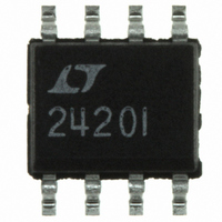
LTC2420IS8#PBF Linear Technology, LTC2420IS8#PBF Datasheet - Page 14

LTC2420IS8#PBF
Manufacturer Part Number
LTC2420IS8#PBF
Description
IC ADC 20BIT MICRPWR W/OSC 8SOIC
Manufacturer
Linear Technology
Datasheet
1.LTC2420CS8.pdf
(36 pages)
Specifications of LTC2420IS8#PBF
Number Of Bits
20
Sampling Rate (per Second)
7.5
Data Interface
MICROWIRE™, Serial, SPI™
Number Of Converters
2
Power Dissipation (max)
1mW
Voltage Supply Source
Single Supply
Operating Temperature
-40°C ~ 85°C
Mounting Type
Surface Mount
Package / Case
8-SOIC (0.154", 3.90mm Width)
Lead Free Status / RoHS Status
Lead free / RoHS Compliant
Available stocks
Company
Part Number
Manufacturer
Quantity
Price
APPLICATIO S I FOR ATIO
LTC2420
Whenever an external clock is not present at the F
converter automatically activates its internal oscillator and
enters the Internal Conversion Clock mode. The LTC2420
operation will not be disturbed if the change of conversion
clock source occurs during the sleep state or during the
data output state while the converter uses an external
serial clock. If the change occurs during the conversion
state, the result of the conversion in progress may be
outside specifications but the following conversions will
not be affected. If the change occurs during the data output
state and the converter is in the Internal SCK mode, the
serial clock duty cycle may be affected but the serial data
stream will remain valid.
Table 3. LTC2420 State Duration
State
CONVERT
SLEEP
DATA OUTPUT
14
Figure 5. LTC2420 Normal Mode Rejection When
Using an External Oscillator of Frequency f
INPUT FREQUENCY DEVIATION FROM NOTCH FREQUENCY (%)
–100
–110
–120
–130
–140
–60
–70
–80
–90
–12
Operating Mode
Internal Oscillator
External Oscillator
Internal Serial Clock
External Serial Clock with
Frequency f
–8
U
–4
SCK
U
0
kHz
4
W
8
2420 F05
F
(60Hz Rejection)
F
(50Hz Rejection)
F
with Frequency f
(f
F
(Internal Oscillator)
F
Frequency f
12
O
O
O
O
O
EOSC
= LOW
= HIGH
= External Oscillator
= LOW/HIGH
= External Oscillator with
EOSC
/2560 Rejection)
U
O
pin, the
EOSC
EOSC
kHz
kHz
Table 3 summarizes the duration of each state as a
function of F
SERIAL INTERFACE
The LTC2420 transmits the conversion results and re-
ceives the start of conversion command through a syn-
chronous 3-wire interface. During the conversion and
sleep states, this interface can be used to assess the
converter status and during the data output state it is used
to read the conversion result.
Serial Clock Input/Output (SCK)
The serial clock signal present on SCK (Pin 7) is used to
synchronize the data transfer. Each bit of data is shifted out
the SDO pin on the falling edge of the serial clock.
In the Internal SCK mode of operation, the SCK pin is an
output and the LTC2420 creates its own serial clock by
dividing the internal conversion clock by 8. In the External
SCK mode of operation, the SCK pin is used as input. The
internal or external SCK mode is selected on power-up and
then reselected every time a HIGH-to-LOW transition is
detected at the CS pin. If SCK is HIGH or floating at power-
up or during this transition, the converter enters the inter-
nal SCK mode. If SCK is LOW at power-up or during this
transition, the converter enters the external SCK mode.
Duration
133ms
160ms
20510/f
As Long As CS = HIGH Until CS = 0 and SCK
As Long As CS = LOW But Not Longer Than 1.26ms
(24 SCK cycles)
As Long As CS = LOW But Not Longer Than 256/f
(24 SCK cycles)
As Long As CS = LOW But Not Longer Than 24/f
(24 SCK cycles)
O
.
EOSC
s
SCK
EOSC
ms
ms


