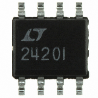
LTC2420IS8#PBF Linear Technology, LTC2420IS8#PBF Datasheet - Page 24

LTC2420IS8#PBF
Manufacturer Part Number
LTC2420IS8#PBF
Description
IC ADC 20BIT MICRPWR W/OSC 8SOIC
Manufacturer
Linear Technology
Datasheet
1.LTC2420CS8.pdf
(36 pages)
Specifications of LTC2420IS8#PBF
Number Of Bits
20
Sampling Rate (per Second)
7.5
Data Interface
MICROWIRE™, Serial, SPI™
Number Of Converters
2
Power Dissipation (max)
1mW
Voltage Supply Source
Single Supply
Operating Temperature
-40°C ~ 85°C
Mounting Type
Surface Mount
Package / Case
8-SOIC (0.154", 3.90mm Width)
Lead Free Status / RoHS Status
Lead free / RoHS Compliant
Available stocks
Company
Part Number
Manufacturer
Quantity
Price
APPLICATIO S I FOR ATIO
LTC2420
For large input capacitor values (C
spikes are averaged by the capacitor into a DC current. The
gain shift becomes a linear function of input source
resistance independent of input capacitance, see Figures
21 and 22. The equivalent input impedance is 16.6M .
This results in 150nA of input dynamic current at the
extreme values of V
V
and full-scale readings for every 10
resistance.
In addition to the input current spikes, the input ESD
protection diodes have a temperature dependent leakage
current. This leakage current, nominally 1nA ( 10nA
max), results in a fixed offset shift of 10 V for a 10k source
resistance.
24
REF
= 5V). This corresponds to a 0.3ppm shift in offset
Figure 20. Full-Scale Error vs R
–10
–20
–30
–40
–50
50
40
20
10
30
10
Figure 19. Offset vs R
0
0
1
1
V
V
V
T
V
V
V
T
A
CC
REF
IN
A
CC
REF
IN
= 25 C
= 25 C
= 0V
= 5V
= 5V
= 5V
= 5V
= 5V
10
10
U
C
C
IN
C
IN
C
IN
C
IN
IN
IN
C
= 1000pF
C
= 1000pF
IN
= 100pF
(V
IN
= 100pF
= 0.01 F
C
100
100
R
R
= 0pF
IN
= 0pF
SOURCE
SOURCE
IN
U
= 0.01 F
= 0V and V
( )
( )
SOURCE
1k
1k
IN
SOURCE
W
10k
10k
(Small C)
> 0.01 F), the input
2420 F19
2420 F20
IN
of input source
(Small C)
100k
100k
= V
REF
U
, when
Reference Current (V
Similar to the analog input, the reference input has a
dynamic input current. This current has negligible effect
on the offset. However, the reference current at V
is similar to the input current at full-scale. For large values
of reference capacitance (C
error shift is 0.03ppm/ of external reference resistance
independent of the capacitance at V
the capacitance tied to V
input resistance of up to 80k (20pF parasitic capacitance
at V
Unlike the analog input, the integral nonlinearity of the
device can be degraded with excessive external RC time
constants tied to the reference input. If the capacitance at
REF
) may be tolerated, see Figure 24.
Figure 22. Full-Scale Error vs R
–20
–25
–35
–15
–30
–10
35
–5
30
25
20
15
10
5
0
Figure 21. Offset vs R
0
5
0
0
V
V
V
T
A
CC
REF
IN
= 25 C
= 0V
= 5V
= 5V
200
200
C
C
C
C
C
C
C
C
C
C
C
C
IN
IN
IN
IN
IN
IN
IN
IN
IN
IN
IN
IN
= 22 F
= 10 F
= 1 F
= 0.1 F
= 0.01 F
= 0.001 F
= 22 F
= 10 F
= 1 F
= 0.1 F
= 0.01 F
= 0.001 F
REF
400
R
400
R
REF
SOURCE
SOURCE
)
VREF
is small (C
600
( )
600
( )
SOURCE
> 0.01 F), the full-scale
SOURCE
V
V
V
T
800
REF
800
CC
REF
IN
A
(Large C)
= 25 C
= 0V
= 5V
VREF
= 5V
2420 F21
, see Figure 23. If
2420 F22
(Large C)
1000
1000
< 0.01 F), an
IN
= V
REF


