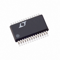
LTC2424IG Linear Technology, LTC2424IG Datasheet - Page 9

LTC2424IG
Manufacturer Part Number
LTC2424IG
Description
IC ADC 20BIT 4CH MICROPWR 28SSOP
Manufacturer
Linear Technology
Datasheet
1.LTC2424CGPBF.pdf
(36 pages)
Specifications of LTC2424IG
Number Of Bits
20
Sampling Rate (per Second)
7.5
Data Interface
MICROWIRE™, Serial, SPI™
Number Of Converters
1
Power Dissipation (max)
1mW
Voltage Supply Source
Single Supply
Operating Temperature
-40°C ~ 85°C
Mounting Type
Surface Mount
Package / Case
28-SSOP (0.200", 5.30mm Width)
Lead Free Status / RoHS Status
Contains lead / RoHS non-compliant
Available stocks
Company
Part Number
Manufacturer
Quantity
Price
Part Number:
LTC2424IG#PBF
Manufacturer:
LINEAR/凌特
Quantity:
20 000
Part Number:
LTC2424IG#TRPBF
Manufacturer:
LINEAR/凌特
Quantity:
20 000
PIN
GND (Pins 1, 6, 16, 18, 22, 27, 28): Ground. Should be
connected directly to a ground plane through a minimum
length trace or it should be the single-point-ground in a
single-point grounding system.
V
5.5V. Bypass to GND with a 10 F tantalum capacitor in
parallel with 0.1 F ceramic capacitor as close to the part
as possible.
FS
full-scale input value. When V
full scale (FFFFF
FS
ADCIN (Pin 4): Analog Input. The input voltage range is
– 0.125 • V
voltage range may be limited by the pin absolute maxi-
mum rating of – 0.3V to V
ZS
zero-scale input value. When V
zero scale (00000
LTC2408 this pin must be grounded.
MUXOUT (Pin 7): MUX Output. This pin is the output of the
multiplexer. Tie to ADCIN for normal operation.
CH0 (Pin 9): Analog Multiplexer Input.
TYPICAL PERFOR A CE CHARACTERISTICS
CC
SET
SET
SET
12
U
20
18
16
14
10
(Pins 2, 8): Positive Supply Voltage. 2.7V
0
INL vs Output Rate
V
V
F
– ZS
(Pin 3): Full-Scale Set Input. This pin defines the
(Pin 5): Zero-Scale Set Input. This pin defines the
FUNCTIONS
O
CC
REF
10 20 30
= EXTERNAL
= 5V
= 5V
U
REF
SET
T
A
.
OUTPUT RATE (Hz)
= –45 C
to 1.125 • V
H
T
40
H
A
). The total reference voltage (V
). For pin compatibility with the LTC2404/
= 25 C
50 60 70 80 90 100
U
CC
REF
T
A
W
= 90 C
+ 0.3V.
IN
. For V
IN
24248 G27
= FS
= ZS
U
SET
SET
REF
, the ADC outputs
, the ADC outputs
> 2.5V the input
20
18
16
14
12
10
0
INL vs Output Rate
V
V
F
T
O
CC
REF
A
10 20 30
= EXTERNAL
= 25 C
= 3V
T
REF
= 2.5V
V
A
= –45 C
CC
) is
OUTPUT RATE (Hz)
40
50 60 70 80 90 100
CH1 (Pin 10): Analog Multiplexer Input.
CH2 (Pin 11): Analog Multiplexer Input.
CH3 (Pin 12): Analog Multiplexer Input.
CH4 (Pin 13): Analog Multiplexer Input. No connect on the
LTC2424.
CH5 (Pin 14): Analog Multiplexer Input. No connect on the
LTC2424.
CH6 (Pin 15): Analog Multiplexer Input. No connect on the
LTC2424.
CH7 (Pin 17): Analog Multiplexer Input. No connect on the
LTC2424.
CLK (Pin 19): Shift Clock for Data In. This clock synchro-
nizes the serial data transfer into the MUX. For normal
operation, drive this pin in parallel with SCK.
CSMUX (Pin 20): MUX Chip Select Input. A logic high on
this input allows the MUX to receive a channel address. A
logic low enables the selected MUX channel and connects
it to the MUXOUT pin for A/D conversion. For normal
operation, drive this pin in parallel with CSADC.
D
is shifted into this input on the last four rising CLK edges
before CSMUX goes low.
IN
(Pin 21): Digital Data Input. The multiplexer address
T
A
= 90 C
24248 G28
LTC2424/LTC2428
24
22
20
18
16
0 7.5
Resolution vs Output Rate
V
V
f
O
CC
REF
= EXTERNAL
= 5V
= 5V
25
OUTPUT RATE (Hz)
50
75
T
T
T
A
A
A
= 25 C
= 90 C
= –45 C
24248 G29
9
100


