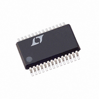
LTC2424IG Linear Technology, LTC2424IG Datasheet - Page 11

LTC2424IG
Manufacturer Part Number
LTC2424IG
Description
IC ADC 20BIT 4CH MICROPWR 28SSOP
Manufacturer
Linear Technology
Datasheet
1.LTC2424CGPBF.pdf
(36 pages)
Specifications of LTC2424IG
Number Of Bits
20
Sampling Rate (per Second)
7.5
Data Interface
MICROWIRE™, Serial, SPI™
Number Of Converters
1
Power Dissipation (max)
1mW
Voltage Supply Source
Single Supply
Operating Temperature
-40°C ~ 85°C
Mounting Type
Surface Mount
Package / Case
28-SSOP (0.200", 5.30mm Width)
Lead Free Status / RoHS Status
Contains lead / RoHS non-compliant
Available stocks
Company
Part Number
Manufacturer
Quantity
Price
Part Number:
LTC2424IG#PBF
Manufacturer:
LINEAR/凌特
Quantity:
20 000
Part Number:
LTC2424IG#TRPBF
Manufacturer:
LINEAR/凌特
Quantity:
20 000
APPLICATIONS
Converter Operation Cycle
The LTC2424/LTC2428 are low power, 4-/8-channel delta-
sigma analog-to-digital converters with easy-to-use
4-wire interfaces. Their operation is simple and made up
of four states. The converter operation begins with the
conversion, followed by a sleep state and concluded with
the data output (see Figure 1). Channel selection may be
performed while the device is in the sleep state or at the
conclusion of the data output state. The interface consists
of serial data output (SDO), serial clock (CLK/SCK), chip
select (CSADC/CSMUX) and data input (D
to CLK and CSADC to CSMUX, the interface requires only
four wires.
Initially, the LTC2424 or LTC2428 performs a conversion.
Once the conversion is complete, the device enters the
sleep state. While in the sleep state if CSADC is high, power
consumption is reduced by an order of magnitude. The
part remains in the sleep state as long as CSADC is logic
HIGH. The conversion result is held indefinitely in a static
shift register while the converter is in the sleep state.
Channel selection for the next conversion cycle is per-
formed while the device is in the sleep state or at the end
of the data output state. A specific channel is selected by
applying a 4-bit serial word to the D
of CLK while CSMUX is HIGH, see Figure 4 and Table 3. The
Figure 1. LTC2428 State Transition Diagram
U
1
(CHANNEL SELECT)
CHANNEL SELECT
DATA OUTPUT
INFORMATION
CONVERT
(SLEEP)
CSADC
U
SLEEP
SCK
AND
0
24248 F01
IN
W
pin on the rising edge
IN
). By tying SCK
U
channel is selected based on the last four bits clocked into
the D
previous channel remains selected.
In the example, Figure 4, the MUX channel is selected
during the sleep state, just before the data output state
begins. Once the channel selection is complete, the device
remains in the sleep state as long as CSADC remains
HIGH.
Once CSADC is pulled low, the device begins outputting
the conversion result. There is no latency in the conversion
result. Since there is no latency, the first conversion
following a change in input channel is valid and corre-
sponds to that channel. The data output corresponds to
the conversion just performed. This result is shifted out on
the serial data output pin (SDO) under the control of the
serial clock (SCK). Data is updated on the falling edge of
SCK allowing the user to reliably latch data on the rising
edge of SCK, see Figure 4. The data output state is
concluded once 24 bits are read out of the ADC or when
CSADC is brought HIGH. The device automatically initiates
a new conversion and the cycle repeats.
Through timing control of the CSADC and SCK pins, the
LTC2424/LTC2428 offer two modes of operation: internal
or external SCK. These modes do not require program-
ming configuration registers; moreover, they do not dis-
turb the cyclic operation described above. These modes of
operation are described in detail in the Serial Interface
Timing Modes section.
Conversion Clock
A major advantage delta-sigma converters offer over
conventional type converters is an on-chip digital filter
(commonly known as Sinc or Comb filter). For high
resolution, low frequency applications, this filter is typi-
cally designed to reject line frequencies of 50 or 60Hz plus
their harmonics. In order to reject these frequencies in
excess of 110dB, a highly accurate conversion clock is
required. The LTC2424/LTC2428 incorporate an on-chip
highly accurate oscillator. This eliminates the need for
external frequency setting components such as crystals or
oscillators. Clocked by the on-chip oscillator, the LTC2424/
LTC2428 reject line frequencies (50 or 60Hz 2%) a
minimum of 110dB.
IN
pin before CSMUX goes low. If D
LTC2424/LTC2428
IN
is all 0’s, the
11


