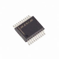
MAX1145BEAP+ Maxim Integrated Products, MAX1145BEAP+ Datasheet - Page 14

MAX1145BEAP+
Manufacturer Part Number
MAX1145BEAP+
Description
IC ADC 14BIT 150KSPS 20-SSOP
Manufacturer
Maxim Integrated Products
Datasheet
1.MAX1144BEAP.pdf
(18 pages)
Specifications of MAX1145BEAP+
Number Of Bits
14
Sampling Rate (per Second)
150k
Data Interface
MICROWIRE™, QSPI™, Serial, SPI™
Number Of Converters
1
Power Dissipation (max)
26.4mW
Voltage Supply Source
Analog and Digital
Operating Temperature
-40°C ~ 85°C
Mounting Type
Surface Mount
Package / Case
20-SSOP
Conversion Rate
150 KSPs
Resolution
14 bit
Interface Type
Serial (3-Wire, SPI, QSPI, Microwire)
Snr
82 dB
Voltage Reference
2.048 V
Supply Voltage (max)
3.465 V
Supply Voltage (min)
3.135 V
Maximum Power Dissipation
640 mW
Maximum Operating Temperature
+ 85 C
Mounting Style
SMD/SMT
Input Voltage
3.3 V
Minimum Operating Temperature
- 40 C
Lead Free Status / RoHS Status
Lead free / RoHS Compliant
magnitude of the offset produced by a synchronous
signal depends on the signal’s shape, recalibration
may be appropriate if the shape or relative timing of the
clock or other digital signals change, which can occur
if more than one clock signal or frequency is used.
Avoid degrading dynamic performance by choosing an
amplifier with distortion much less than the
MAX1144/MAX1145’s THD (-90dB) at frequencies of
interest. If the chosen amplifier has insufficient com-
mon-mode rejection, which results in degraded THD
performance, use the inverting configuration to elimi-
nate errors from common-mode voltage. Low tempera-
ture-coefficient resistors reduce linearity errors caused
by resistance changes due to self-heating. Also, to
reduce linearity errors due to finite amplifier gain, use
an amplifier circuit with sufficient loop gain at the fre-
quencies of interest.
If DC accuracy is important, choose a buffer with an
offset much less than the MAX1144/MAX1145’s maxi-
mum offset (±6mV), or whose offset can be trimmed
while maintaining good stability over the required tem-
perature range.
The MAX1144/MAX1145 are fully compatible with
MICROWIRE and SPI/QSPI devices. MICROWIRE and
SPI/QSPI both transmit a byte and receive a byte at the
same time. The simplest software interface requires
only three 8-bit transfers to perform a conversion (one
8-bit transfer to configure the ADC, and two more 8-bit
transfers to clock out the 14-bit conversion result).
Configure short acquisition by setting M1 = 0 and M0 =
0. In short acquisition mode, the acquisition time is 5
clock cycles. The total period is 24 clock cycles per
conversion.
Configure long acquisition by setting M1 = 1 and M0 =
1. In long acquisition mode, the acquisition time is 13
clock cycles. The total period is 32 clock cycles per
conversion.
A calibration is initiated through the serial interface by
setting M1 = 0 and M0 = 1. Calibration can be done in
either internal or external clock mode, though it is desir-
able that the part be calibrated in the same mode in
which it will be used to do conversions. The part
remains in calibration mode for approximately 80,000
14-Bit ADCs, 150ksps, 3.3V Single Supply
14
______________________________________________________________________________________
Operating Modes and Serial Interfaces
Short Acquisition Mode (24 SCLK)
Long Acquisition Mode (32 SCLK)
Calibration Mode
DC Accuracy
Distortion
clock cycles unless the calibration is aborted. Calibr-
ation is halted if RST or SHDN goes low, or if a valid
start condition occurs.
A software power-down is initiated by setting M1 = 1
and M0 = 0. After the conversion completes, the part
shuts down. It reawakens upon receiving a new start
bit. Conversions initiated with M1 = 1 and M0 = 0 (shut-
down) use the acquisition mode selected for the previ-
ous conversion.
The MAX1144/MAX1145 may be shut down by pulling
SHDN low or by asserting software shutdown. In addi-
tion to lowering power dissipation to 4µW, considerable
power can be saved by shutting down the conv-
erter for short periods between conversions. There is
no need to perform a calibration after the converter has
been shut down unless the time in shutdown is long
enough that the supply voltage or ambient temperature
may have changed.
For best system performance, use separate analog and
digital ground planes. The two ground planes should
be tied together at the MAX1144/MAX1145. Use pin 3
and pin 14 as the primary AGND and DGND, respec-
tively. If the analog and digital supplies come from the
same source, isolate the digital supply from the analog
with a low-value resistor (10Ω).
The MAX1144/MAX1145 are not sensitive to the order
of AV
present in the absence of the other. Do not apply an
external reference voltage until after both AV
DV
Be sure that digital return currents do not pass through
the analog ground. All return-current paths must be low
impedance. A 5mA current flowing through a PC board
ground trace impedance of only 0.05Ω creates an error
voltage of about 250µV, or about 0.5LSBs error with a
±4V full-scale system. The board layout should ensure
that digital and analog signal lines are kept separate.
Do not run analog and digital lines parallel to one
another. If you must cross one with the other, do so at
right angles.
The ADC is sensitive to high-frequency noise on the
AV
ground plane with 0.1µF. If the main supply is not ade-
quately bypassed, add an additional 1µF or 10µF low-
ESR capacitor in parallel with the primary bypass
capacitor.
DD
DD
DD
are present.
power supply. Bypass this supply to the analog
and DV
DD
Supplies, Layout, Grounding,
sequencing. Either supply can be
Software Shutdown
Shutdown Mode
and Bypassing
DD
and


