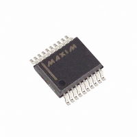
MAX1145BEAP+ Maxim Integrated Products, MAX1145BEAP+ Datasheet - Page 13

MAX1145BEAP+
Manufacturer Part Number
MAX1145BEAP+
Description
IC ADC 14BIT 150KSPS 20-SSOP
Manufacturer
Maxim Integrated Products
Datasheet
1.MAX1144BEAP.pdf
(18 pages)
Specifications of MAX1145BEAP+
Number Of Bits
14
Sampling Rate (per Second)
150k
Data Interface
MICROWIRE™, QSPI™, Serial, SPI™
Number Of Converters
1
Power Dissipation (max)
26.4mW
Voltage Supply Source
Analog and Digital
Operating Temperature
-40°C ~ 85°C
Mounting Type
Surface Mount
Package / Case
20-SSOP
Conversion Rate
150 KSPs
Resolution
14 bit
Interface Type
Serial (3-Wire, SPI, QSPI, Microwire)
Snr
82 dB
Voltage Reference
2.048 V
Supply Voltage (max)
3.465 V
Supply Voltage (min)
3.135 V
Maximum Power Dissipation
640 mW
Maximum Operating Temperature
+ 85 C
Mounting Style
SMD/SMT
Input Voltage
3.3 V
Minimum Operating Temperature
- 40 C
Lead Free Status / RoHS Status
Lead free / RoHS Compliant
Figure 7. AIN Buffer for AC/DC Use
Clocking in a control byte starts input acquisition. The
main capacitor array starts acquiring the input as soon
as a start bit is recognized, using the same input range
as the previous conversion. If the opposite input range
is selected by the second DIN bit, the part immediately
switches to the new sampling mode. Acquisition time is
one-and-a-half clock cycles shorter when switching
from unipolar to bipolar or bipolar to unipolar modes
than when continuously converting in the same mode.
Acquisition can be extended by eight clock cycles by
setting M1 = 1 and M0 = 1 (long acquisition mode). The
sampling instant in short acquisition completes on the
falling edge of the sixth clock cycle after the start bit
(Figure 2). Acquisition is 5 clock cycles in short acquisi-
tion mode and 13 clock cycles in long acquisition
mode. Short acquisition mode is 24 clock cycles per
conversion. Using the external clock to run the conver-
sion process limits unipolar conversion speed to
125ksps instead of 150ksps as in bipolar mode. The
input resistance in unipolar mode is larger than that of
bipolar mode (Figure 1). The RC time constant in unipo-
lar mode is larger than that of bipolar mode, reducing
the maximum conversion rate in 24 external clock
mode. Long acquisition mode with external clock
allows both unipolar and bipolar sampling of 112ksps
as (3.6MHz / 32 clock cycles) by adding eight extra
clock cycles to the conversion.
Most applications require an input buffer amplifier. If
the input signal is multiplexed, the input channel should
be switched immediately after acquisition, rather than
near the end of or after a conversion. This allows more
time for the input buffer amplifier to respond to a large
step change in input signal. The input amplifier must
14-Bit ADCs, 150ksps, 3.3V Single Supply
______________________________________________________________________________________
Input Acquisition and Settling
IN
2
3
V
V
CC
EE
7
4
6
0.1µF
0.1µF
100pF
1kΩ
1kΩ
have a high enough slew rate to complete the required
output voltage change before the beginning of the
acquisition time.
At the beginning of acquisition, the capacitive DAC is
connected to the amplifier output, causing some output
disturbance. Ensure that the sampled voltage has set-
tled to within the required limits before the end of the
acquisition time. If the frequency of interest is low, AIN
can be bypassed with a large enough capacitor to
charge the capacitive DAC with very little change in
voltage. However, for AC use, AIN must be driven by a
wideband buffer (at least 10MHz), which must be sta-
ble with the DAC’s capacitive load (in parallel with any
AIN bypass capacitor used) and also must settle quickly
(Figure 7).
Digital noise can couple to AIN and REF. The conver-
sion clock (SCLK) and other digital signals that are
active during input acquisition contribute noise to the
conversion result. If the noise signal is synchronous to
the sampling interval, an effective input offset is pro-
duced. Asynchronous signals produce random noise
on the input, whose high-frequency components may
be aliased into the frequency band of interest. Minimize
noise by presenting a low impedance (at the frequen-
cies contained in the noise signal) at the inputs. This
requires bypassing AIN to AGND, or buffering the input
with an amplifier that has a small-signal bandwidth of
several MHz, or preferably both. AIN has a bandwidth
of about 4MHz.
Offsets resulting from synchronous noise (such as the
conversion clock) are canceled by the MAX1144/
MAX1145’s calibration scheme. However, because the
0.0033µF
AIN
Digital Noise
13


