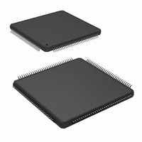
ADC08D500CIYB/NOPB National Semiconductor, ADC08D500CIYB/NOPB Datasheet - Page 6

ADC08D500CIYB/NOPB
Manufacturer Part Number
ADC08D500CIYB/NOPB
Description
IC ADC 8BIT 500MSPS DUAL 128LQFP
Manufacturer
National Semiconductor
Series
PowerWise®r
Specifications of ADC08D500CIYB/NOPB
Number Of Bits
8
Sampling Rate (per Second)
500M
Data Interface
Serial
Number Of Converters
2
Power Dissipation (max)
1.78W
Voltage Supply Source
Single Supply
Operating Temperature
-40°C ~ 85°C
Mounting Type
Surface Mount
Package / Case
128-LQFP Exposed Pad
Lead Free Status / RoHS Status
Lead free / RoHS Compliant
Other names
*ADC08D500CIYB
*ADC08D500CIYB/NOPB
ADC08D500CIYB
*ADC08D500CIYB/NOPB
ADC08D500CIYB
Available stocks
Company
Part Number
Manufacturer
Quantity
Price
Company:
Part Number:
ADC08D500CIYB/NOPB
Manufacturer:
Texas Instruments
Quantity:
10 000
Pin Functions
Pin No.
127
126
18
19
11
10
22
23
31
7
.
CalDly / DES /
Symbol
CalRun
V
V
CLK+
V
CLK-
V
V
SCS
V
IN
IN
CMO
IN
IN
BG
.
Q+
Q−
I+
I−
Equivalent Circuit
5
Calibration Delay, Dual Edge Sampling and Serial Interface Chip
Select. With a logic high or low on pin 14, this pin functions as
Calibration Delay and sets the number of clock cycles after power
up before calibration begins (See Section 1.1.1). With pin 14
floating, this pin acts as the enable pin for the serial interface input
and the CalDly value becomes 0b (short delay with no provision
for a long power-up calibration delay). When this pin is floating or
connected to a voltage equal to V
mode is selected where the "I" input is sampled at twice the clock
rate and the "Q" input is ignored. See Section 1.1.5.1.
LVDS Clock input pins for the ADC. The differential clock signal
must be a.c. coupled to these pins. The input signal is sampled on
the falling edge of CLK+. See Section 1.1.2 for a description of
acquiring the input and Section 2.3 for an overview of the clock
inputs.
Analog signal inputs to the ADC. The differential full-scale input
range is 650 mV
the FSR pin is high.
Common Mode Voltage. This pin is the common mode output in
d.c. coupling mode and also serves as the a.c. coupling mode
select pin. When d.c. coupling is used, the voltage output at this
pin is required to be the common mode input voltage at V
V
when a.c. coupling is used at the analog inputs. This pin is capable
of sourcing or sinking 100 μA. See Section 2.2.
Bandgap output voltage capable of 100 μA source/sink.
Calibration Running indication. This pin is at a logic high when
calibration is running.
IN
− when d.c. coupling is used. This pin should be grounded
P-P
when the FSR pin is low, or 870 mV
Description
A
/2, DES (Dual Edge Sampling)
www.national.com
P-P
IN
+ and
when


