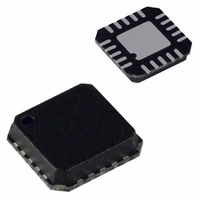
AD7986BCPZ Analog Devices Inc, AD7986BCPZ Datasheet - Page 5

AD7986BCPZ
Manufacturer Part Number
AD7986BCPZ
Description
IC ADC 18BIT 2MSPS SAR 20LFCSP
Manufacturer
Analog Devices Inc
Datasheet
1.AD7986BCPZ.pdf
(28 pages)
Specifications of AD7986BCPZ
Data Interface
MICROWIRE™, QSPI™, Serial, SPI™
Number Of Bits
18
Sampling Rate (per Second)
2M
Number Of Converters
1
Power Dissipation (max)
34mW
Voltage Supply Source
Analog and Digital
Operating Temperature
-40°C ~ 85°C
Mounting Type
Surface Mount
Package / Case
20-VFQFN, CSP Exposed Pad
Resolution (bits)
18bit
Sampling Rate
2MSPS
Input Channel Type
Differential
Supply Voltage Range - Analog
2.375V To 2.625V
Digital Ic Case Style
CSP
No. Of Pins
20
Lead Free Status / RoHS Status
Lead free / RoHS Compliant
Available stocks
Company
Part Number
Manufacturer
Quantity
Price
Company:
Part Number:
AD7986BCPZ
Manufacturer:
Allen Bradlley
Quantity:
100
Company:
Part Number:
AD7986BCPZ
Manufacturer:
Analog Devices Inc
Quantity:
135
TIMING SPECIFICATIONS
AVDD = DVDD = 2.5 V, BVDD = 5 V, VIO = 1.8 V to 2.7 V, V
Table 4.
Parameter
Conversion Time: CNV Rising Edge to Data Available (Turbo Mode/Normal Mode)
Acquisition Time
Time Between Conversions (Turbo Mode/Normal Mode)
CNV Pulse Width (CS Mode)
Data Read During Conversion (Turbo Mode/Normal Mode)
Quiet Time During Acquisition from Last SCK Falling Edge to CNV Rising Edge
SCK Period (CS Mode)
SCK Period (Chain Mode)
SCK Low Time
SCK High Time
SCK Falling Edge to Data Remains Valid
SCK Falling Edge to Data Valid Delay
CNV or SDI Low to SDO D17 MSB Valid (CS Mode)
CNV or SDI High or Last SCK Falling Edge to SDO High Impedance (CS Mode)
SDI Valid Setup Time from CNV Rising Edge
SDI Valid Hold Time from CNV Rising Edge (CS Mode)
SDI Valid Hold Time from CNV Rising Edge (Chain Mode)
SCK Valid Setup Time from CNV Rising Edge (Chain Mode)
SCK Valid Hold Time from CNV Rising Edge (Chain Mode)
SDI Valid Setup Time from SCK Falling Edge (Chain Mode)
SDI Valid Hold Time from SCK Falling Edge (Chain Mode)
SDI High to SDO High (Chain Mode with Busy Indicator)
1
See Figure 2 and Figure 3 for load conditions.
Figure 2. Load Circuit for Digital Interface Timing
TO SDO
20pF
C
L
500µA
500µA
I
I
OL
OH
1.4V
Rev. B | Page 5 of 28
REF
= 4.096 V, T
A
1
= −40°C to +85°C, unless otherwise noted.
MINIMUM V
SPECIFICATIONS IN TABLE 3.
90% VIO
t
DELAY
Symbol
t
t
t
t
t
t
t
t
t
t
t
t
t
t
t
t
t
t
t
t
t
t
CONV
ACQ
CYC
CNVH
DATA
QUIET
SCK
SCK
SCKL
SCKH
HSDO
DSDO
EN
DIS
SSDICNV
HSDICNV
HSDICNV
SSCKCNV
HSCKCNV
SSDISCK
HSDISCK
DSDOSDI
IH
AND MAXIMUM V
Figure 3. Voltage Levels for Timing
V
V
IH
IL
1
1
Min
100
500/660
10
20
9
11
3.5
3.5
2
4
0
0
5
5
2
3
IL
USED. SEE DIGITAL INPUTS
Typ
10% VIO
t
DELAY
V
V
Max
400/500
200/300
6
10
8
5
IH
IL
1
1
1
AD7986
Unit
ns
ns
ns
ns
ns
ns
ns
ns
ns
ns
ns
ns
ns
ns
ns
ns
ns
ns
ns
ns
ns
ns


