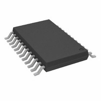
AD7367BRUZ-5 Analog Devices Inc, AD7367BRUZ-5 Datasheet - Page 5

AD7367BRUZ-5
Manufacturer Part Number
AD7367BRUZ-5
Description
IC ADC 14BIT DUAL 500KSPS 24-TSS
Manufacturer
Analog Devices Inc
Datasheet
1.AD7367BRUZ-5.pdf
(28 pages)
Specifications of AD7367BRUZ-5
Data Interface
DSP, MICROWIRE™, QSPI™, Serial, SPI™
Design Resources
Driving the AD7366/7 Bipolar SAR ADC in Low-Distortion DC-Coupled Appls (CN0042)
Number Of Bits
14
Sampling Rate (per Second)
500k
Number Of Converters
2
Power Dissipation (max)
88.8mW
Voltage Supply Source
Analog and Digital, Dual ±
Operating Temperature
-40°C ~ 85°C
Mounting Type
Surface Mount
Package / Case
24-TSSOP (0.173", 4.40mm Width)
Resolution (bits)
14bit
Input Channel Type
Single Ended
Supply Voltage Range - Analogue
4.75V To 5.25V, ± 11.5V To ± 16.5V
Supply Voltage Range - Digital
2.7V To
Sampling Rate
1MSPS
Rohs Compliant
Yes
Lead Free Status / RoHS Status
Lead free / RoHS Compliant
For Use With
EVAL-AD7367CBZ - BOARD EVALUATION FOR AD7367
Lead Free Status / RoHS Status
Lead free / RoHS Compliant, Lead free / RoHS Compliant
Available stocks
Company
Part Number
Manufacturer
Quantity
Price
Company:
Part Number:
AD7367BRUZ-5
Manufacturer:
ADI
Quantity:
1 000
Company:
Part Number:
AD7367BRUZ-5-RL7
Manufacturer:
ADI
Quantity:
1 000
AD7367-5 SPECIFICATIONS
AV
V
Table 3.
Parameter
DYNAMIC PERFORMANCE
SAMPLE AND HOLD
DC ACCURACY
ANALOG INPUT
REF
Signal-to-Noise Ratio (SNR)
Signal-to-Noise (+ Distortion) Ratio (SINAD)
Total Harmonic Distortion (THD)
Spurious-Free Dynamic Range (SFDR)
Intermodulation Distortion (IMD)
Channel-to-Channel Isolation
Aperture Delay
Aperture Jitter
Aperture Delay Matching
Full Power Bandwidth
Resolution
Integral Nonlinearity (INL)
Differential Nonlinearity (DNL)
Positive Full-Scale Error
Positive Full-Scale Error Match
Zero Code Error
Zero Code Error Match
Negative Full-Scale Error
Negative Full-Scale Error Match
Input Voltage Ranges
DC Leakage Current
Input Capacitance
Input Impedance
CC
= 2.5 V internal/external; T
Second-Order Terms
Third-Order Terms
(Programmed via RANGE Pins)
= DV
CC
= 4.75 V to 5.25 V; V
2
2
1
1
1
1
2
1
1
1
1
A
1
1
= −40°C to +85°C, unless otherwise noted.
1
DD
1
= 5 V to 16.5 V; V
1
1
Min
74
73
14
SS
= −16.5 V to −5 V; V
Rev. A | Page 5 of 28
Typ
76
75
−84
−87
−91
−89
−90
40
±100
35
8
±2
±0.5
±4
±5
±3
±0.2
±1
±5
±3
±0.2
±4
±5
±3
±0.2
±0.01
9
13
500
2.5
250
1.2
Max
−78
−79
10
±3.5
±0.90
±25
±25
±10
±25
±25
±25
±10
±5
0 to 10
±1
DRIVE
Unit
dB
dB
dB
dB
dB
dB
dB
ns
ps
ps
MHz
MHz
Bits
LSB
LSB
LSB
LSB
LSB
LSB
LSB
LSB
LSB
LSB
LSB
LSB
LSB
LSB
V
V
V
μA
pF
pF
kΩ
MΩ
kΩ
MΩ
= 2.7 V to 5.25 V; f
Test Conditions/Comments
f
fa = 49 kHz, fb = 51 kHz
@ 3 dB, ±10 V range
@ 0.1 dB, ±10 V range
Guaranteed no missed codes to 14 bits
±5 V and ±10 V analog input range
0 V to 10 V analog input range
Matching from ADC A to ADC B
Channel-to-channel matching for ADC A and ADC B
±5 V and ±10 V analog input range
0 V to 10 V analog input range
Matching from ADC A to ADC B
Channel-to-channel matching for ADC A and ADC B
±5 V and ±10 V analog input range
0 V to 10 V analog input range
Matching from ADC A to ADC B
Channel-to-channel matching for ADC A and ADC B
See Table 7
When in track, ±10 V range
When in track, ±5 V or 0 V to +10 V range
For ±10 V @ 500 kSPS
For ±10 V @ 100 kSPS
For ±5 V/0 V to +10 V @ 500 kSPS
For ±5 V/0 V to +10 V @ 100 kSPS
IN
= 50 kHz sine wave
SAMPLE
AD7366-5/AD7367-5
= 500 kSPS; f
SCLK
= 20 MHz;


