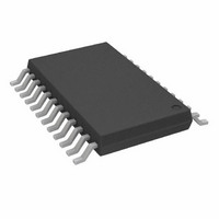
AD7367BRUZ-5 Analog Devices Inc, AD7367BRUZ-5 Datasheet - Page 18

AD7367BRUZ-5
Manufacturer Part Number
AD7367BRUZ-5
Description
IC ADC 14BIT DUAL 500KSPS 24-TSS
Manufacturer
Analog Devices Inc
Datasheet
1.AD7367BRUZ-5.pdf
(28 pages)
Specifications of AD7367BRUZ-5
Data Interface
DSP, MICROWIRE™, QSPI™, Serial, SPI™
Design Resources
Driving the AD7366/7 Bipolar SAR ADC in Low-Distortion DC-Coupled Appls (CN0042)
Number Of Bits
14
Sampling Rate (per Second)
500k
Number Of Converters
2
Power Dissipation (max)
88.8mW
Voltage Supply Source
Analog and Digital, Dual ±
Operating Temperature
-40°C ~ 85°C
Mounting Type
Surface Mount
Package / Case
24-TSSOP (0.173", 4.40mm Width)
Resolution (bits)
14bit
Input Channel Type
Single Ended
Supply Voltage Range - Analogue
4.75V To 5.25V, ± 11.5V To ± 16.5V
Supply Voltage Range - Digital
2.7V To
Sampling Rate
1MSPS
Rohs Compliant
Yes
Lead Free Status / RoHS Status
Lead free / RoHS Compliant
For Use With
EVAL-AD7367CBZ - BOARD EVALUATION FOR AD7367
Lead Free Status / RoHS Status
Lead free / RoHS Compliant, Lead free / RoHS Compliant
Available stocks
Company
Part Number
Manufacturer
Quantity
Price
Company:
Part Number:
AD7367BRUZ-5
Manufacturer:
ADI
Quantity:
1 000
Company:
Part Number:
AD7367BRUZ-5-RL7
Manufacturer:
ADI
Quantity:
1 000
AD7366-5/AD7367-5
Unlike other bipolar ADCs, the AD7366-5/AD7367-5 do not
have a resistive analog input structure. On the AD7366-5/
AD7366-5, the bipolar analog signal is sampled directly onto
the sampling capacitor. This gives the devices high analog input
impedance. The analog input impedance can be calculated from
the following formula:
where:
f
C
C
Inputs section). When operating at 500 kSPS, the analog input
impedance is typically 260 kΩ for the ±10 V range. As the
sampling frequency is reduced, the analog input impedance
further increases. As the analog input impedance increases, the
current required to drive the analog input therefore, decreases
(see Figure 7 for more information).
S
S
S
is the sampling frequency.
is the sampling capacitor value.
depends on the analog input range chosen (see the Analog
Z = 1/(f
S
× C
S
)
+5V TO +16.5V
–16.5V TO –5V
ANALOG INPUTS ±10V,
±5V, AND 0V TO +10V
SUPPLY
SUPPLY
Figure 20. Typical Connection Diagram for ±10 V Range Using Internal Reference
680nF
+
680nF
+
+
10µF
10µF
+
+
0.1µF
+
V
V
V
V
D
D
0.1µF
A1
A2
B1
B2
CAP
CAP
V
A
B
V
AD7366-5/
Rev. A | Page 18 of 28
AD7367-5
DD
SS
DV
AGND
CC
RANGE0
RANGE1
REFSEL
AV
CNVST
V
D
D
DGND
ADDR
SCLK
BUSY
DRIVE
CC
OUT
OUT
+
CS
TYPICAL CONNECTION DIAGRAM
Figure 20 shows a typical connection diagram for the AD7366-5/
AD7367-5. In this configuration, the AGND pin is connected
to the analog ground plane of the system, and the DGND pin
is connected to the digital ground plane of the system. The
analog inputs on the AD7366-5/AD7367-5 accept bipolar
single-ended signals. The AD7366-5/AD7367-5 can operate
with either an internal or an external reference. In Figure 20, the
AD7366-5/AD7367-5 is configured to operate with the internal
2.5 V reference. A 680 nF decoupling capacitor is required when
operating with the internal reference.
The AV
The V
input structures. The voltage on these pins must be greater than
or equal to ±5 V (see Table 7 for more information). The V
is connected to the supply voltage of the microprocessor. The
voltage applied to the V
serial interface. V
0.1µF
A
B
+
0.1µF
0.1µF
DD
CC
V
and V
DRIVE
and DV
+
+
10µF
10µF
SS
+3V OR +5V SUPPLY
are the dual supplies for the high voltage analog
CC
DRIVE
+
pins are connected to a 5 V supply voltage.
SERIAL
INTERFACE
+5V SUPPLY
can be set to 3 V or 5 V.
DRIVE
input controls the voltage of the
DRIVE
pin


