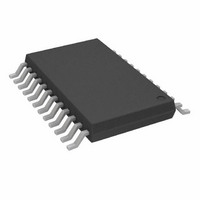
AD7367BRUZ-5 Analog Devices Inc, AD7367BRUZ-5 Datasheet - Page 10

AD7367BRUZ-5
Manufacturer Part Number
AD7367BRUZ-5
Description
IC ADC 14BIT DUAL 500KSPS 24-TSS
Manufacturer
Analog Devices Inc
Datasheet
1.AD7367BRUZ-5.pdf
(28 pages)
Specifications of AD7367BRUZ-5
Data Interface
DSP, MICROWIRE™, QSPI™, Serial, SPI™
Design Resources
Driving the AD7366/7 Bipolar SAR ADC in Low-Distortion DC-Coupled Appls (CN0042)
Number Of Bits
14
Sampling Rate (per Second)
500k
Number Of Converters
2
Power Dissipation (max)
88.8mW
Voltage Supply Source
Analog and Digital, Dual ±
Operating Temperature
-40°C ~ 85°C
Mounting Type
Surface Mount
Package / Case
24-TSSOP (0.173", 4.40mm Width)
Resolution (bits)
14bit
Input Channel Type
Single Ended
Supply Voltage Range - Analogue
4.75V To 5.25V, ± 11.5V To ± 16.5V
Supply Voltage Range - Digital
2.7V To
Sampling Rate
1MSPS
Rohs Compliant
Yes
Lead Free Status / RoHS Status
Lead free / RoHS Compliant
For Use With
EVAL-AD7367CBZ - BOARD EVALUATION FOR AD7367
Lead Free Status / RoHS Status
Lead free / RoHS Compliant, Lead free / RoHS Compliant
Available stocks
Company
Part Number
Manufacturer
Quantity
Price
Company:
Part Number:
AD7367BRUZ-5
Manufacturer:
ADI
Quantity:
1 000
Company:
Part Number:
AD7367BRUZ-5-RL7
Manufacturer:
ADI
Quantity:
1 000
AD7366-5/AD7367-5
Pin No.
18
19
20
21
22
24
Mnemonic
REFSEL
CS
SCLK
CNVST
BUSY
DGND
Description
Internal/External Reference Selection, Logic Input. If this pin is tied to logic high, the on-chip 2.5 V reference is
used as the reference source for both ADC A and ADC B. In addition, Pin D
decoupling capacitors. If the REFSEL pin is tied to GND, an external reference can be supplied to the AD7366-5/
AD7367-5 through the D
Chip Select, Active Low Logic Input. This input frames the serial data transfer. When CS is logic low, the output bus
is enabled, and the conversion result is output on D
Serial Clock, Logic Input. A serial clock input provides the SCLK for accessing the data from the AD7366-5/AD7367-5.
Conversion Start, Logic Input. This pin is edge triggered. On the falling edge of this input, the track/hold goes into
hold mode and the conversion is initiated. If CNVST is low at the end of a conversion, the part goes into power-
down mode. In this case, the rising edge of CNVST instructs the part to power up again.
Busy Output. BUSY transitions high when a conversion starts and remains high until the conversion completes.
Digital Ground. This is the ground reference point for all digital circuitry on the AD7366-5/AD7367-5. The DGND
pin should connect to the DGND plane of a system. The DGND and AGND voltages should ideally be at the same
potential and must not be more than 0.3 V apart, even on a transient basis.
CAP
A and/or D
Rev. A | Page 10 of 28
CAP
B pins.
OUT
A and D
OUT
B.
CAP
A and Pin D
CAP
B must be tied to


