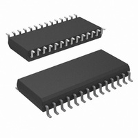
LM9822CCWM/NOPB National Semiconductor, LM9822CCWM/NOPB Datasheet - Page 8

LM9822CCWM/NOPB
Manufacturer Part Number
LM9822CCWM/NOPB
Description
IC SCANNER COLOR ANALOG 28-SOIC
Manufacturer
National Semiconductor
Datasheet
1.LM9822CCWMXNOPB.pdf
(22 pages)
Specifications of LM9822CCWM/NOPB
Number Of Bits
14
Number Of Channels
3
Power (watts)
375mW
Voltage - Supply, Analog
5V
Voltage - Supply, Digital
3V, 5V
Package / Case
28-SOIC (7.5mm Width)
Lead Free Status / RoHS Status
Lead free / RoHS Compliant
Other names
*LM9822CCWM
*LM9822CCWM/NOPB
LM9822CCWM
*LM9822CCWM/NOPB
LM9822CCWM
Pin Descriptions
V
V
V
AGND
V
DGND
OS
MCLK
VSMP
CLMP
REF+
REF-
A
D
R
,
,
OS
V
REFMID
G
,
OS
,
B
The two
They should be connected to a voltage
source of +5V and bypassed to
0.1µF monolithic capacitor in parallel with a
10µF tantalum capacitor.
These two pins are the ground returns for
the analog supplies.
This is the positive supply pin for the digital
I/O pins. It should be connected to a voltage
source between +3.3V and +5.0V and be
bypassed to DGND with a 0.1µF monolithic
capacitor in parallel with a 10µF tantalum
capacitor.
This is the ground return for the digital sup-
ply.
Analog Inputs. These inputs (for Red,
Green, and Blue) should be tied to the sen-
sor’s OS (Output Signal) through DC block-
ing capacitors.
Voltage reference bypass pins. V
V
bypassed to
lithic capacitor.
Master clock input. The ADC conversion
rate will be 1/2 of MCLK. 12MHz is the max-
imum frequency for MCLK.
Sample timing input signal. If VSMP is high
on the rising edge of MCLK, the input is
sampled on the rising edge of the next
MCLK. The reference signal for the next
pixel will be sampled one to four MCLKs
later, depending on the value in the
CDSREF configuration bits. If CDS is not
enabled, the internal reference will be sam-
pled during the reference sample time.
The number of MCLK cycles between
VSMP pulses determines the pixel rate.
Timing Diagrams 1 through 6 illustrate the
VSMP timings for all the valid pixel rates.
Note: See the applications section of the
datasheet for the proper timing relationships
between VSMP and MCLK.
Clamp timing input. If CLMP and VSMP are
high on the rising edge of MCLK, all three
OS inputs will be internally connected to
V
VREF+ or VREF- depending on the state of
the Signal Polarity bit in the Sample Mode
register (Reg. 0, Bit 4).
CLAMP
REFMID
Analog Input/Output
Timing Control
Analog Power
during the next pixel.
, and V
A
pins are the analog supply pins.
AGND
REF-
through a 0.1uF mono-
should each be
V
CLAMP
AGND
REF+
is either
with a
,
8
Connection Diagram
D7
SCLK
SDO
SDI
SEN
-
D0
V
BANDGAP
V
REFMID
AGND
AGND
V
V
SDO
REF+
OS
SEN
OS
OS
REF-
SDI
V
V
G
A
R
B
A
10
11
12
13
14
4
1
2
3
5
6
7
8
9
Data Output pins. The 14 bit conversion
results of the ADC are multiplexed in 8 bit
bytes to
The MSB consists of data bits d13-d6 on
pins D7-D0 and the LSB consists of d5-d0
on pins D7-D3 with D1 and D0 low.
Serial Shift Clock. Input data on SDI is valid
on the rising edge of SCLK. The minimum
SCLK period is 1 t
Serial Data Output. Data bits are shifted out
of SDO on falling edges of SCLK. The first
eight falling edges of SCLK after SEN goes
low will shift out eight data bits (MSB first)
from the configuration register addressed
during the previous SEN low time.
Serial Data Input. A read/write bit, followed
by a four address bits and eight data bits is
shifted into SDI, MSB first. Data should be
valid on the rising edge of SCLK. If the
read/write bit is a “0” (a write), then the
shifted data bits will be stored. If the
read/write bit is a “1” (a read), then the data
bits will be ignored, and SDO will shift out
the addressed register’s contents during the
next SEN low time.
Shift enable and load signal. When SEN is
low, data is shifted into SDI. When SEN
goes high, the last thirteen bits (one
read/write, four address and eight data)
shifted into SDI will be used to program the
addressed configuration register. SEN must
be high for at least 3 MCLK cycles between
SEN low times.
Serial Input/Output
Data Output
LM9822
28 pin
D7
SOIC
-
D0
synchronous with MCLK.
MCLK
.
28
27
24
22
21
20
19
18
17
16
15
26
25
23
www.national.com
D7
D6
D5
D4
D3
D2
D1
V
CLMP
D0
DGND
VSMP
MCLK
SCLK
D


