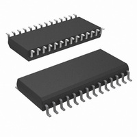
LM9822CCWM/NOPB National Semiconductor, LM9822CCWM/NOPB Datasheet - Page 21

LM9822CCWM/NOPB
Manufacturer Part Number
LM9822CCWM/NOPB
Description
IC SCANNER COLOR ANALOG 28-SOIC
Manufacturer
National Semiconductor
Datasheet
1.LM9822CCWMXNOPB.pdf
(22 pages)
Specifications of LM9822CCWM/NOPB
Number Of Bits
14
Number Of Channels
3
Power (watts)
375mW
Voltage - Supply, Analog
5V
Voltage - Supply, Digital
3V, 5V
Package / Case
28-SOIC (7.5mm Width)
Lead Free Status / RoHS Status
Lead free / RoHS Compliant
Other names
*LM9822CCWM
*LM9822CCWM/NOPB
LM9822CCWM
*LM9822CCWM/NOPB
LM9822CCWM
Applications Information
pling point for particular CCD sensors. Diagram 7 shows how the
various settings of CDSREF can be used to delay the Reference
Sampling point. Care must be taken to avoid setting CDSREF to
an inappropriate value when operating in the lower “Divide By”
modes.
Valid CDSREF settings are:
9.7 PD (Power Down) Mode
A Power Down bit is provided to configure the LM9822 in a lower
power “StandBy” mode. In this mode, typical power consumption
is reduced to less than 1% of normal operating power. The serial
interface is still active, but the majority of the analog and digital
circuitry is powered down.
10.0 LM9822 Basic Operation
The normal operational sequence when using the LM9822 is as
follows:
Immediately after applying power, all configuration registers are
reset to default settings. MCLK should be applied, and the appro-
priate values written to the registers using the procedure dis-
cussed in section 8.0 Serial Interface and Configuration Registers
on page 20 and detailed in Diagrams 10, 11 and 12. Once the
configuration registers are loaded, the timing control signals can
be applied at the proper rates for the mode of conversion desired.
MCLK is applied initially with VSMP and CLMP low. After at least
3 MCLKS, VSMP and CLMP signals can begin. The Divide By
mode is determined by the ratio of MCLK to VSMP frequency as
described in section 10.2.
14-Bit conversion results are placed on the data output pins as
follows: The upper 8 bits are output first with bit 13 of the ADC on
D7 and the bit 6 of the ADC on D0. The lower 6 bits are then out-
put with bit 5 of the ADC on D7 and bit 0 of the ADC on D2. D0
and D1 are always 0 when the lower 6 bits of data are being out-
put. The exact timing and conversion latency of the output data is
affected by the settings of the DOE variable in the Sample Mode
register, and the Divide By mode of operation. If DOE = 0 (recom-
mended setting for best performance), output data will change on
the falling edge of MCLK. If DOE = 1, output data is updated on
the rising edge of MCLK. See Diagrams 1 through 6 and Diagram
13 for more information on data output timing.
10.1 CLMP Operation
The CLMP signal is used to engage the LM9822 internal clamp
circuits at the proper time during the CCD or CIS data output
cycle. If both CLMP and VSMP are high on a rising edge of
MCLK, then CLMP will be applied during the next pixel. The exact
timing of the internal Clamp signal is determined by the Divide By
mode of operation and the setting of the SMPCL variable in the
Sample Mode register. If SMPCL = 0, then the Clamp is on for 1
“Divide By” Mode
/8
/6
/3
/2
Valid CDSREF
00,01,10,11
00,01,10,11
(Continued)
00,01
00
21
MCLK before the reference is sampled. If SMPCL = 1 then the
clamp is on between the reference and the signal sample points.
Please see Diagram 8 and Diagram 9 for a graphic example of
this timing.
To clamp across multiple pixels in a row, CLMP can be set high
and remain there for the entire number of pixels to be clamped,
then returned to the low state for normal (signal) operation. This
may simplify the timing required to generate the CLMP signal.
10.2 MCLK and VSMP Timing
The relationship between VSMP and MCLK is used to determine
the 'Divide By' mode that is presently being used with the part.
Valid 'Divide By' settings are:
Color - /8, /6
Monochrome - /8, /6, /3, /2
When entering a new mode, it is important to provide consistent
MCLK/VSMP timing signals that meet the following condition.
When switching to a new 'Divide By' mode, VSMP should be held
low for a minimum of 3 MCLK cycles, then valid timing according
to the datasheet diagrams for the particular mode should be
started. This ensures that all internal circuitry is properly synchro-
nized to the new conversion 'Divide By' mode being used. If the
timing relationship between VSMP and MCLK is disturbed for any
reason, the same procedure should be used before restarting
operation in the chosen 'Divide By' mode.
For example: To change from monochrome Divide By 3 mode to
monochrome Divide By 2 mode, VSMP should be held low for at
least 3 MCLK cycles, then VSMP can be brought high using
"Divide By 2" timing. If VSMP is not low for at least 3 MCLKs, the
LM9822 may enter an unknown mode.
MCLK
VSMP
Figure 6: Timing of Transitions between ‘Divide By’ Modes
Divide by 3
Transition
( 3 MCLK)
www.national.com
Divide by 2


