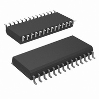
LM9822CCWM/NOPB National Semiconductor, LM9822CCWM/NOPB Datasheet - Page 18

LM9822CCWM/NOPB
Manufacturer Part Number
LM9822CCWM/NOPB
Description
IC SCANNER COLOR ANALOG 28-SOIC
Manufacturer
National Semiconductor
Datasheet
1.LM9822CCWMXNOPB.pdf
(22 pages)
Specifications of LM9822CCWM/NOPB
Number Of Bits
14
Number Of Channels
3
Power (watts)
375mW
Voltage - Supply, Analog
5V
Voltage - Supply, Digital
3V, 5V
Package / Case
28-SOIC (7.5mm Width)
Lead Free Status / RoHS Status
Lead free / RoHS Compliant
Other names
*LM9822CCWM
*LM9822CCWM/NOPB
LM9822CCWM
*LM9822CCWM/NOPB
LM9822CCWM
Applications Information
5.0 Offset DAC
The Offset DACs remove the DC offsets generated by the sensor
and the LM9822’s analog signal chain (see section 5.1, Internal
Offsets). The DAC value for each color (registers 1,2 and 3)
should be set during calibration to the lowest value that still
results in an ADC output code greater than zero for all the pixels
when scanning a black line. With a PGA gai n of 1V/V, each LSB
of the offset DAC typically adds the equivalent of 20 ADC LSBs,
providing a total offset adjustment range of ±590 ADC LSBs. The
Offset DAC’s output voltage is given by:
In terms of 12 bit output codes, the offset is given by:
The offset is positive if bit B5 is cleared and negative if B5 is set.
Since the analog offset is added before the PGA gain, the value
of the PGA gain must be considered when selecting the offset
DAC values.
5.1 Internal Offsets
Figure 4 is a model of the LM9822’s internal offsets. Equation 4
shows how to calculate the expected output code given the input
voltage (V
the programmed offset DAC voltage (V
gains (G
C is a constant that combines the gain error through the AFE, ref-
erence voltage variance, and analog voltage to digital code con-
version into one constant. Ideally, C = 2048 codes/V (4096
codes/2V) in 12 bit LSBs. Manufacturing tolerances widen the
range of C (see Electrical Specifications).
Equation 5 is a simplification of the output code calculation,
neglecting the LM9822’s internal offsets.
D
Equation 4: Output code calculation with internal offsets
V
OUT
IN
Offse
Equation 5: Simplified output code calculation
V
+
=
B
+
OS1
, G
Equation 3: Offset in ADC Output Codes
IN
Equation 2: Offset DAC Output Voltage
), the LM9822 internal offsets (
PGA
V
x3 Boost
V
1V/V or
=
G
DAC
3V/V
IN
D
t20L SBs(value in B4 - B0) PGA Gain
B
Figure 4: Internal Offset Model
) and the analog channel gain constant C.
O UT
+
V
=
O S1
+
V
=
9.75mV (value in B4 - B0)
+
OS2
V
G
IN
+
Offset
B
DAC
+
G
+
V
B
0.93V/V to
V
DAC
+
DAC
G
PGA
3V/V
V
PGA
DAC
+
V
DAC
V
+
OS2
G
(Continued)
+
OS3
PGA
), the programmed
OS1
G
C
PG A
ADC
, V
OS2
+
V
, V
OS3
D
OUT
OS3
C
),
18
6.0 Clamping
To perform a DC restore across the AC coupling capacitors at the
beginning of every line, the LM9822 implements a clamping func-
tion. The clamping function is initiated by asserting the CLMP
input. If CLMP and VSMP are both high on a rising edge of
MCLK, all three OS inputs will be internally connected to
V
is set to one (positive signal polarity), then the OS input will be
connected to
then it will be connected to
6.1 Clamp Capacitor Selection
The output signal of many sensors rides on a DC offset (greater
than 5V for many CCDs) which is incompatible with the LM9822’s
5V operation. To eliminate this offset without resorting to addi-
tional higher voltage components, the output of the sensor is AC
coupled to the LM9822 through a DC blocking capacitor, C
The sensor’s DOS output, if available, is not used. The value of
this capacitor is determined by the leakage current of the
LM9822’s OS input and the output impedance of the sensor. The
leakage through the OS input determines how quickly the capaci-
tor value will drift from the clamp value of
then determines how many pixels can be processed before the
droop causes errors in the conversion (±0.1V is the recom-
mended limit for CDS operation). The output impedance of the
sensor determines how quickly the capacitor can be charged to
the clamp value during the black reference period at the begin-
ning of every line.
The minimum clamp capacitor value is determined by the maxi-
mum droop the LM9822 can tolerate while converting one sensor
line. The minimum clamp capacitor value is much smaller for CDS
mode applications than it is for CIS mode applications.
The LM9822 input current is considerably less when the LM9822
is operating in CDS mode. In CDS mode, the LM9822 average
input current is no more than 25nA. With CDS disabled, which will
likely be the case when CIS sensors are used, the LM9822 input
impedance will be 1/(f
rate of the analog input and C
REF-
during the next pixel, depending on bit 4 of register 0. If bit 4
V
V
IN
IN
V
C
C
REF-
CLAMP
CLAMP
. If bit 4 is set to zero (negative signal polarity),
OS C
OS
Figure 5: Input Circuitry
CDS Mode Input Circuitry
CIS Mode Input Circuitry
Sample
Vref
Inside LM9822
Inside LM9822
P2
S
V
REF+
*C
S
is 2pF.
P1
P1
S
.
C
P2
). where f
S
+
+
C
C
I
I
Sample
V
REF+
www.national.com
or
is the sample
V
REF-
V
, which
REF+
CLAMP
or
.


