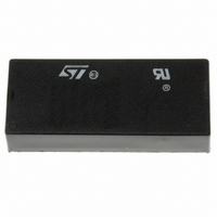
M48T128Y-70PM1 STMicroelectronics, M48T128Y-70PM1 Datasheet - Page 8

M48T128Y-70PM1
Manufacturer Part Number
M48T128Y-70PM1
Description
IC TIMEKPR NVRAM 1MBIT 5V 32-DIP
Manufacturer
STMicroelectronics
Series
Timekeeper®r
Type
Clock/Calendar/NVSRAMr
Datasheet
1.M48T128Y-70PM1.pdf
(23 pages)
Specifications of M48T128Y-70PM1
Memory Size
1M (128K x 8)
Time Format
HH:MM:SS (24 hr)
Date Format
YY-MM-DD-dd
Interface
Parallel
Voltage - Supply
4.5 V ~ 5.5 V
Operating Temperature
0°C ~ 70°C
Mounting Type
Through Hole
Package / Case
32-DIP (600 mil) Module
Function
Clock, Calendar, NV Timekeeping RAM, Battery Backup
Rtc Memory Size
1 MB
Supply Voltage (max)
4.5 V to 5.5 V
Supply Voltage (min)
4.5 V
Maximum Operating Temperature
+ 70 C
Minimum Operating Temperature
0 C
Mounting Style
Through Hole
Rtc Bus Interface
Parallel
Lead Free Status / RoHS Status
Lead free / RoHS Compliant
Other names
497-2834-5
Available stocks
Company
Part Number
Manufacturer
Quantity
Price
Operation modes
2.1
Figure 4.
Note:
Table 3.
1. Valid for ambient operating temperature: T
2. C
8/23
Symbol
t
t
t
t
GHQZ
GLQX
EHQZ
ELQX
t
t
t
t
t
L
GLQV
AXQX
AVQV
ELQV
AVAV
= 5 pF.
(2)
(2)
(2)
(2)
READ mode
The M48T128Y/V is in the READ mode whenever W (WRITE enable) is high and E (chip
enable) is low. The unique address specified by the 17 address inputs defines which one of
the 131,072 bytes of data is to be accessed.
Valid data will be available at the data I/O pins within t
last address input signal is stable, providing the E and G access times are also satisfied. If
the E and G access times are not met, valid data will be available after the latter of the chip
enable access times (t
three-state data I/O signals is controlled by E and G. If the outputs are activated before
t
are changed while E and G remain active, output data will remain valid for t
data hold time) but will go indeterminate until the next address access.
READ mode AC waveforms
WE = High.
READ mode AC characteristics
AVQV
READ cycle time
Address valid to output valid
Chip enable low to output valid
Output enable low to output valid
Chip enable low to output transition
Output enable low to output transition
Chip enable high to output Hi-Z
Output enable high to output Hi-Z
Address transition to output transition
A0-A16
E
G
DQ0-DQ7
, the data lines will be driven to an indeterminate state until t
Parameter
ELQV
A
tAVQV
tELQX
= 0 to 70 °C; V
tGLQX
tELQV
) or output enable access time (t
(1)
tGLQV
Doc ID 5746 Rev 6
tAVAV
VALID
CC
= 4.5 to 5.5 V or 3.0 to 3.6 V (except where noted).
DATA OUT
Min
70
10
M48T128Y
5
5
tAXQX
AVQV
–70
tGHQZ
Max
70
70
40
25
25
(address access time) after the
GLQV
). The state of the eight
AVQV
Min
85
M48T128Y, M48T128V
M48T128V
5
5
5
tEHQZ
. If the address inputs
–85
AXQX
Max
85
85
55
30
30
(output
AI01197
Unit
ns
ns
ns
ns
ns
ns
ns
ns
ns


