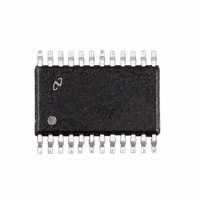
LMX2352TMX/NOPB National Semiconductor, LMX2352TMX/NOPB Datasheet - Page 3

LMX2352TMX/NOPB
Manufacturer Part Number
LMX2352TMX/NOPB
Description
IC FREQ SYNTHESIZER DUAL 24TSSOP
Manufacturer
National Semiconductor
Series
PLLatinum™r
Type
PLL Frequency Synthesizerr
Datasheet
1.LMX2352TMNOPB.pdf
(21 pages)
Specifications of LMX2352TMX/NOPB
Pll
Yes with Bypass
Input
CMOS, TTL
Output
CMOS
Number Of Circuits
1
Ratio - Input:output
3:3
Differential - Input:output
Yes/No
Frequency - Max
1.2GHz, 550MHz
Divider/multiplier
Yes/No
Voltage - Supply
2.7 V ~ 5.5 V
Operating Temperature
-40°C ~ 85°C
Mounting Type
Surface Mount
Package / Case
24-TSSOP
Frequency-max
1.2GHz
Lead Free Status / RoHS Status
Lead free / RoHS Compliant
Other names
LMX2352TMX
LMX2352TMXTR
LMX2352TMXTR
Available stocks
Company
Part Number
Manufacturer
Quantity
Price
Company:
Part Number:
LMX2352TMX/NOPB
Manufacturer:
ST
Quantity:
7 600
Pin Descriptions
Package
for CSP
Pin No.
10
11
12
13
14
15
16
17
18
19
20
21
22
23
9
package
Pin No.
TSSOP
for
10
11
12
13
14
15
16
17
18
19
20
21
22
23
24
Pin Name
OSCin
FoLD
RF_EN
IF_EN
CLOCK
DATA
LE
GND
fin IF
fin IF
GND
CPo
Vp
Vcc
OUT1
IF
IF
IF
(Continued)
I/O
O
O
O
I
I
I
I
I
I
-
I
I
-
-
-
Multiplexed output of N or R divider and RF/IF lock detect. Active High/Low CMOS
RF PLL Enable. Powers down RF N and R counters, prescaler, and will TRI-STATE
Description
Oscillator input which can be configured to drive both the IF and RF R counter inputs
or only the IF R counter depending on the state of the OSC programming bit. (See
functional description 1.1 and programming description 3.1.)
output except in analog lock detect mode. (See programming description 3.1.5.)
the charge pump output when LOW. Bringing RF_EN high powers up RF PLL
depending on the state of RF_CTL_WORD. (See functional description 1.9.)
IF PLL Enable. Powers down IF N and R counters, prescaler, and will TRI-STATE the
charge pump output when LOW. Bringing IF_EN high powers up IF PLL depending on
the state of IF_CTL_WORD. (See functional description 1.9.)
High impedance CMOS Clock input. Data for the various counters is clocked into the
24 - bit shift register on the rising edge.
Binary serial data input. Data entered MSB first. The last two bits are the control bits.
High impedance CMOS input.
Load enable high impedance CMOS input. Data stored in the shift registers is loaded
into one of the 4 internal latches when LE goes HIGH. (See functional description 1.7.)
Ground for IF analog circuitry.
IF prescaler complimentary input. A bypass capacitor should be placed as close as
possible to this pin and be connected directly to the ground plane.
IF prescaler input. Small signal input from the VCO.
Ground for IF digital circuitry.
IF charge pump output. For connection to a loop filter for driving the input of an
external VCO.
Power supply for IF charge pump. Must be
IF power supply voltage input. Must be equal to Vcc
5.5 V. Bypass capacitors should be placed as close as possible to this pin and be
connected directly to the ground plane.
Programmable CMOS output. Level of the output is controlled by IF_N [18] bit.
3
V
cc RF
and V
RF
. Input may range from 2.7 V to
cc IF
.
www.national.com
®


