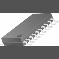
LMX2352TM National Semiconductor, LMX2352TM Datasheet

LMX2352TM
Specifications of LMX2352TM
Available stocks
Related parts for LMX2352TM
LMX2352TM Summary of contents
Page 1
... LMX2350/2352 via a three wire interface (Data, LE, Clock). Supply voltage can range from 2 5.5 V. The LMX2350/ Block Diagram © 2001 National Semiconductor Corporation LMX2352 family features very low current consumption; typi- cally LMX2350 (2.5 GHz) 6.5 mA, LMX2352 (1.2 GHz) 4. 3.0V. The LMX2350/2352 are available in a 24-pin TSSOP and 24-pin CSP surface mount plastic package ...
Page 2
... OSCx I/O www.national.com DS100831-2 Order Number LMX2350TM or LMX2352TM NS Package Number MTC24 DS100831-22 Description Programmable CMOS output. Level of the output is controlled by IF_N [17] bit. RF PLL power supply voltage input. Must be equal to Vcc 5.5 V. Bypass capacitors should be placed as close as possible to this pin and be connected directly to the ground plane ...
Page 3
Pin Descriptions (Continued) Pin No. Pin No. Pin Name I/O for CSP for Package TSSOP package 9 10 OSCin FoLD RF_EN IF_EN CLOCK DATA I ...
Page 4
... Absolute Maximum Ratings If Military/Aerospace specified devices are required, please contact the National Semiconductor Sales Office/ Distributors for availability and specifications. Parameter Power Supply Voltage Voltage on any pin with GND = 0 volts Storage Temperature Range Lead Temperature (Solder 4 sec.) Recommended Operating Conditions Parameter ...
Page 5
Electrical Characteristics specified) (Continued) All Min/Max specifications are guaranteeed by design, or test, or statistical methods. Symbol Parameter Charge Pump ICPo- RF Charge Pump source Output Current (see RF Programming ICPo- sink RF Description 3.2.2) ICPo- source RF ICPo- sink ...
Page 6
Charge Pump Current Specification Definitions sink current − sink current Vp sink current ...
Page 7
RF Sensitivity Test Block Diagram Note 10,000 Note: Sensitivity limit is reached when the error of the divided RF output, F Typical Performance Characteristics LMX2350 I TRI-STATE ...
Page 8
Typical Performance Characteristics Charge Pump Current vs CP Voltage O RF_CP_WORD = 0011 and 1111 RF Input Impedance V = 2.7V to 5.5V MHz GHz (f Capacitor = 100 pF) IN www.national.com (Continued) ...
Page 9
Typical Performance Characteristics LMX2350 RF Sensitivity vs Frequency IF Input Sensitivity vs Frequency LMX2350 V Voltage vs V Load Current in Vdoubler P P Mode 25˚C (Continued) LMX2352 RF Sensitivity vs Frequency DS100831-17 Oscillator Input Sensitivity vs Frequency ...
Page 10
... General The basic phase-lock-loop (PLL) configuration consists of a high-stability crystal reference oscillator, a frequency synthe- sizer such as the National Semiconductor LMX2350/52, a voltage controlled oscillator (VCO), and a passive loop filter. The frequency synthesizer includes a phase detector, cur- rent mode charge pump, as well as programmable reference [R] and feedback [N] frequency dividers ...
Page 11
Functional Description and 3.2.2). The phase detector also receives a feedback signal from the charge pump, in order to eliminate dead zone. 1.5 Charge Pump The phase detector’s current source outputs pump charge into an external loop filter, which then ...
Page 12
Programming Description 2.0 INPUT DATA REGISTER The descriptions below describe the 24-bit data register loaded through the MICROWIRE Interface. The data register is used to program the 15-bit IF_R counter register, and the 15-bit RF_R counter register, the 15-bit IF_N ...
Page 13
Programming Description 3.1.3 15-BIT PROGRAMMABLE REFERENCE DIVIDER RATIO (R COUNTER) Divide Ratio 32,767 Notes: Divide ratio 32,767 (Divide ratios less ...
Page 14
Programming Description 3.2.1 (RF_R [22 - 23] ) DLL_MODE V2_EN BIT LOCATION DLL_MODE RF_R [23] V2_EN RF_R [22] 1. V2_EN bit when set high enables the voltage doubler for the RF Charge Pump supply. 2. DLL_MODE bit should be set ...
Page 15
Programming Description 4.1.2 3-BIT IF SWALLOW COUNTER DIVIDE RATIO (IF A COUNTER) Swallow Count ( Note: Swallow Counter Value IF_NB_CNTR IF_NA_CNTR Minimum continuous count = 56 ( A=0, B=7) 4.1.3 12-BIT IF PROGRAMMABLE ...
Page 16
Programming Description Synchronous Power down Mode One of the PLL loops can be synchronously powered down by first setting the power down mode bit HIGH (IF_N[21 and then asserting its power down bit (IF_N[22] or RF_N[22] = 1). ...
Page 17
Programming Description 4.4.1 Programmable CMOS Output Truth Table BIT LOCATION OUT_0 IF_N[17] OUT_1 IF_N[18] FastLock IF_N[20] When the FastLock bit is set to one, OUT_0 and OUT_1 are don’t care bits. FastLock mode utilizes the OUT0 and OUT1 output pins ...
Page 18
Programming Description 4.6 LOCK DETECT DIGITAL FILTER The Lock Detect Digital Filter compares the difference between the phase of the inputs of the phase detector generated delay of approximately 15nS. To enter the locked state (Lock = ...
Page 19
Programming Description 4.7 ANALOG LOCK DETECT FILTER When the Fo/LD output is configured in analog lock detect mode an external lock detect circuit is needed in order to provide a steady LOW signal when the PLL is in the locked ...
Page 20
... Physical Dimensions www.national.com inches (millimeters) unless otherwise noted Molded TSSOP, JEDEC Plastic Package (MTC24) Order Number LMX2350TM or LMX2352TM NS Package MTC24 20 ...
Page 21
... NATIONAL’S PRODUCTS ARE NOT AUTHORIZED FOR USE AS CRITICAL COMPONENTS IN LIFE SUPPORT DEVICES OR SYSTEMS WITHOUT THE EXPRESS WRITTEN APPROVAL OF THE PRESIDENT AND GENERAL COUNSEL OF NATIONAL SEMICONDUCTOR CORPORATION. As used herein: 1. Life support devices or systems are devices or systems which, (a) are intended for surgical implant ...


