LMX2470SLEX National Semiconductor, LMX2470SLEX Datasheet - Page 24
LMX2470SLEX
Manufacturer Part Number
LMX2470SLEX
Description
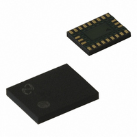
IC PLL DELTA-SIGMA 24LAMUCSP
Manufacturer
National Semiconductor
Type
PLL Frequency Synthesizer, Delta Sigmar
Datasheet
1.LMX2470SLEXNOPB.pdf
(36 pages)
Specifications of LMX2470SLEX
Pll
Yes with Bypass
Input
CMOS
Output
CMOS
Number Of Circuits
1
Ratio - Input:output
3:3
Differential - Input:output
Yes/No
Frequency - Max
2.6GHz
Divider/multiplier
Yes/Yes
Voltage - Supply
2.25 V ~ 2.75 V
Operating Temperature
-40°C ~ 85°C
Mounting Type
Surface Mount
Package / Case
24-Laminate UTCSP
Frequency-max
2.6GHz
For Use With
LMX2470EVAL - EVALUATION BOARD FOR LMX2470
Lead Free Status / RoHS Status
Lead free / RoHS Compliant
Other names
*LMX2470SLEX
*LMX2470SLEX/NOPB
LMX2470SLEXCT
*LMX2470SLEX/NOPB
LMX2470SLEXCT
Available stocks
Company
Part Number
Manufacturer
Quantity
Price


www.national.com
Programming Description
2.0 GENERAL PROGRAMMING INFORMATION
The descriptions below describe the 24-bit data registers loaded through the MICROWIRE Interface. These data registers are
used to program the R counter, the N counter, and the internal mode control latches. The data format of a typical 24-bit data
register is shown below. The control bits CTL [3:0] decode the register address. On the rising edge of LE, data stored in the shift
register is loaded into one of the appropriate latches (selected by address bits). Data is shifted in MSB first. Note that it is best
to program the N counter last, since doing so initializes the digital lock detector and Fastlock circuitry. Note that initialize means
it resets the counters, but it does NOT program values into these registers. Upon a cold power-up, it is necessary to program all
the registers. The exception is when 22-bit is not being used. In this case, it is not necessary to program the R7 register.
2.0.1 Register Location Truth Table
The control bits CTL [2:0] decode the internal register address. The table below shows how the control bits are mapped to the
target control register.
2.0.2 Control Register Content Map
Because the LMX2470 registers are complicated, they are organized into two groups, basic and advanced. The first four registers
are basic registers that contain critical information necessary for the PLL to achieve lock. The last 5 registers are for features that
optimize spur, phase noise, and lock time performance. The next page shows these registers.
MSB
23
C3
x
0
0
0
0
1
1
1
1
DATA [21:0]
C2
x
0
0
1
1
0
0
1
1
4
C1
0
1
0
1
0
1
0
1
x
3
24
C0
0
1
1
1
1
1
1
1
1
2
CTL [3:0]
1
DATA Location
R0
R1
R2
R3
R4
R5
R6
R7
R8
LSB
0
Related parts for LMX2470SLEX
Image
Part Number
Description
Manufacturer
Datasheet
Request
R

Part Number:
Description:
2.6 Ghz Delta-sigma Fractional-n Pll With 800 Mhz Integer-n Pll
Manufacturer:
National Semiconductor Corporation
Datasheet:

Part Number:
Description:
National Semiconductor [8-Bit D/A Converter]
Manufacturer:
National Semiconductor
Datasheet:
Part Number:
Description:
National Semiconductor [Media Coprocessor]
Manufacturer:
National Semiconductor
Datasheet:
Part Number:
Description:
Digitally Controlled Tone and Volume Circuit with Stereo Audio Power Amplifier, Microphone Preamp Stage and National 3D Sound
Manufacturer:
National Semiconductor
Datasheet:
Part Number:
Description:
Digitally Controlled Tone and Volume Circuit with Stereo Audio Power Amplifier, Microphone Preamp Stage and National 3D Sound
Manufacturer:
National Semiconductor
Datasheet:
Part Number:
Description:
AC97 Rev 2 Codec with Sample Rate Conversion and National 3D Sound
Manufacturer:
National Semiconductor
Part Number:
Description:
Manufacturer:
National Semiconductor
Datasheet:
Part Number:
Description:
Manufacturer:
National Semiconductor
Datasheet:
Part Number:
Description:
General Purpose, Low Voltage, Low Power, Rail-to-Rail Output Operational Amplifiers
Manufacturer:
National Semiconductor
Datasheet:
Part Number:
Description:
8-bit 20 MSPS flash A/D converter.
Manufacturer:
National Semiconductor
Datasheet:
Part Number:
Description:
Low Noise Quad Operational Amplifier
Manufacturer:
National Semiconductor
Datasheet:
Part Number:
Description:
Quad Differential Line Receivers
Manufacturer:
National Semiconductor
Datasheet:
Part Number:
Description:
Quad High Speed Trapezoidal? Bus Transceiver
Manufacturer:
National Semiconductor
Datasheet:
Part Number:
Description:
Dual Line Receiver
Manufacturer:
National Semiconductor
Datasheet: