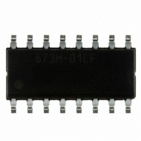
ICS673M-01LF IDT, Integrated Device Technology Inc, ICS673M-01LF Datasheet - Page 6

ICS673M-01LF
Manufacturer Part Number
ICS673M-01LF
Description
IC PLL BUILDING BLOCK 16-SOIC
Manufacturer
IDT, Integrated Device Technology Inc
Type
Phase Lock Loop (PLL)r
Datasheet
1.ICS673M-01LFT.pdf
(8 pages)
Specifications of ICS673M-01LF
Pll
Yes
Input
Clock
Output
Clock
Number Of Circuits
1
Ratio - Input:output
1:2
Differential - Input:output
No/No
Frequency - Max
120MHz
Divider/multiplier
Yes/No
Voltage - Supply
3.135 V ~ 5.5 V
Operating Temperature
0°C ~ 70°C
Mounting Type
Surface Mount
Package / Case
16-SOIC
Frequency-max
120MHz
Number Of Elements
1
Operating Supply Voltage (typ)
3.3/5V
Operating Temp Range
0C to 70C
Package Type
SOIC N
Output Frequency Range
Up to 120MHz
Operating Supply Voltage (min)
3.13V
Operating Supply Voltage (max)
5.25V
Operating Temperature Classification
Commercial
Pin Count
16
Lead Free Status / RoHS Status
Lead free / RoHS Compliant
Other names
673M-01LF
800-1094
800-1094-5
800-1094
800-1094
800-1094-5
800-1094
Available stocks
Company
Part Number
Manufacturer
Quantity
Price
Company:
Part Number:
ICS673M-01LF
Manufacturer:
MICROCHIP
Quantity:
578
MDS 673-01 L
might be 0.5 V below VDD. Hysteresis should be added
to the circuit by connecting R4.
The CLK output frequency may be up to 2x the
maximum Output Clock Frequency listed in the AC
Electrical Characteristics above when the device is in
an unlocked condition. Make sure that the external
divider can operate up to this frequency.
Figure 3. Example Configuration -- Generating a 20 MHz clock from a 200 kHz reference.
200 kHz
Figure 2. Using an External Comparator
R
R
2
3
0.01 F
CHGP VCOIN
to Reset the VCO
REFIN
FBIN
+3.3 or 5 V
R
Z
SEL
200 kHz
C
R
2
4
C
-
+
OE PD
CAP
1
such as ICS674-01
Digital Divider
PD
VDD
100
ICS673-01
w w w. i d t . c o m
6
VCOIN
Explanation of Operation
The ICS673-01 is a PLL building block circuit that
includes an integrated VCO with a wide operating
range. The device uses external PLL loop filter
components which through proper configuration allow
for low input clock reference frequencies, such as a
15.7 kHz Hsync input.
The phase/frequency detector compares the falling
edges of the clocks inputted to FBIN and REFIN. It then
generates an error signal to the charge pump, which
produces a charge proportional to this error. The
external loop filter integrates this charge, producing a
voltage that then controls the frequency of the VCO.
This process continues until the edges of FBIN are
aligned with the edges of the REFIN clock, at which
point the output frequency will be locked to the input
frequency.
R
Z
C
2
GND
C
1
CAP
CLK2
CLK1
PLL B
UILDING
20 MHz
40 MHz
Revision 051310
ICS673-01
B
LOCK


