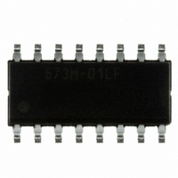
ICS673M-01LF IDT, Integrated Device Technology Inc, ICS673M-01LF Datasheet - Page 2

ICS673M-01LF
Manufacturer Part Number
ICS673M-01LF
Description
IC PLL BUILDING BLOCK 16-SOIC
Manufacturer
IDT, Integrated Device Technology Inc
Type
Phase Lock Loop (PLL)r
Datasheet
1.ICS673M-01LFT.pdf
(8 pages)
Specifications of ICS673M-01LF
Pll
Yes
Input
Clock
Output
Clock
Number Of Circuits
1
Ratio - Input:output
1:2
Differential - Input:output
No/No
Frequency - Max
120MHz
Divider/multiplier
Yes/No
Voltage - Supply
3.135 V ~ 5.5 V
Operating Temperature
0°C ~ 70°C
Mounting Type
Surface Mount
Package / Case
16-SOIC
Frequency-max
120MHz
Number Of Elements
1
Operating Supply Voltage (typ)
3.3/5V
Operating Temp Range
0C to 70C
Package Type
SOIC N
Output Frequency Range
Up to 120MHz
Operating Supply Voltage (min)
3.13V
Operating Supply Voltage (max)
5.25V
Operating Temperature Classification
Commercial
Pin Count
16
Lead Free Status / RoHS Status
Lead free / RoHS Compliant
Other names
673M-01LF
800-1094
800-1094-5
800-1094
800-1094
800-1094-5
800-1094
Available stocks
Company
Part Number
Manufacturer
Quantity
Price
Company:
Part Number:
ICS673M-01LF
Manufacturer:
MICROCHIP
Quantity:
578
MDS 673-01 L
Pin Assignment
Pin Descriptions
V C O IN
Number
C H G P
F B IN
G N D
G N D
G N D
V D D
V D D
Pin
1 6 p in n a rro w (1 5 0 m il) S O IC
10
11
12
13
14
15
16
1
2
3
4
5
6
7
8
9
1
2
3
4
5
6
7
8
VCOIN
Name
CHGP
REFIN
CLK2
CLK1
FBIN
GND
GND
GND
VDD
VDD
CAP
SEL
Pin
OE
NC
PD
1 6
1 5
1 4
1 3
1 2
1 1
1 0
9
Output
Output
Output
Power
Power
Power
Power
Power
Type
Input
Input
Input
Input
Input
Input
Input
Pin
-
R E F IN
N C
C L K 1
C L K 2
P D
S E L
O E
C A P
Feedback clock input. Connect the feedback clock to this pin. Falling
edge triggered.
Connect to +3.3 V or +5 V and to VDD on pin 3.
Connect to VDD on pin 2.
Connect to ground.
Connect to ground.
Connect to ground.
Charge pump output. Connect to VCOIN under normal operation.
Input to internal VCO.
Loop filter return.
Output enable. Active when high. Tri-states both outputs when low.
Select pin for VCO predivide to feedback divider per table above.
Power down. Turns off entire chip when pin is low. Outputs stop low.
Clock output 2. Low skew divide by two version of CLK1.
Clock output 1.
No connect. Nothing is connected internally to this pin.
Reference input. Connect reference clock to this pin. Falling edge is
triggered.
w w w. i d t . c o m
2
VCO Predivide Select Table
0 = connect pin directly to ground
1 = connect pin directly to VDD
Pin Description
SEL
0
1
PLL B
VCO Predivide
UILDING
4
1
Revision 051310
ICS673-01
B
LOCK


