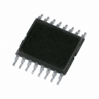
74HCT9046APW,112 NXP Semiconductors, 74HCT9046APW,112 Datasheet - Page 27

74HCT9046APW,112
Manufacturer Part Number
74HCT9046APW,112
Description
IC PLL W/BAND GAP VCO 16-TSSOP
Manufacturer
NXP Semiconductors
Type
Phase Lock Loop (PLL)r
Series
74HCTr
Datasheet
1.74HCT9046AD118.pdf
(43 pages)
Specifications of 74HCT9046APW,112
Number Of Circuits
1
Package / Case
16-TSSOP
Pll
Yes
Input
Clock
Output
Clock
Ratio - Input:output
2:2
Differential - Input:output
No/No
Frequency - Max
16MHz
Divider/multiplier
No/No
Voltage - Supply
4.5 V ~ 5.5 V
Operating Temperature
-40°C ~ 125°C
Mounting Type
Surface Mount
Frequency-max
16MHz
Supply Voltage (max)
5.5 V
Supply Voltage (min)
4.5 V
Maximum Operating Temperature
+ 125 C
Minimum Operating Temperature
- 40 C
Mounting Style
SMD/SMT
Operating Supply Voltage
4.5 V to 5.5 V
Lead Free Status / RoHS Status
Lead free / RoHS Compliant
Other names
568-2914-5
935221200112
935221200112
NXP Semiconductors
13. Application information
Table 7.
Table 8.
74HCT9046A_6
Product data sheet
Component
R1
R2
R1 + R2
C1
Subject
VCO frequency
without extra
offset
VCO frequency
with extra offset
PLL conditions with
no signal at pin
SIG_IN
Survey of components
Design considerations for VCO section
Phase comparator
PC1, PC2
PC1
PC2
PC1, PC2
PC1, PC2
PC1
PC2
This information is a guide for the approximation of values of external components to be
used with the 74HCT9046A in a phase-locked-loop system.
Values of the selected components should be within the ranges shown in
Value
between 3 k and 300 k
between 3 k and 300 k
parallel value > 2.7 k
> 40 pF
Rev. 06 — 15 September 2009
Design consideration
VCO frequency characteristic. With R2 =
3 k < R1 < 300 k , the characteristics of the VCO operation will be as
shown in
when R2 =
Selection of R1 and C1. Given f
Figure
Given f
Figure 33
VCO frequency characteristic. With R1 and R2 within the ranges
3 k < R1 < 300 k < R2 < 300 k , the characteristics of the VCO
operation is as shown in
Selection of R1, R2 and C1. Given f
R1C1 by using
Obtain the values of C1 and R2 by using
R1 from the value of C1 and the product R1C1.
VCO adjusts to f
VCO adjusts to f
31.
max
Figure
to obtain 2f
and f
Figure
).
0
0
offset
29a. (Due to R1, C1 time constant a small offset remains
determine the values of R1 and C1 using
with
L
with
33. Calculate f
and then use this to calculate f
PC_IN
Figure
PC_IN
= 90 and V
0
29b.
, determine the values of R1 and C1 using
= 360 and V
PLL with band gap controlled VCO
0
and f
off
from the equation f
Figure
L
VCO_IN
determine the value of product
and R1 within the range
74HCT9046A
VCO_IN
32. Calculate the value of
= 0.5V
min
© NXP B.V. 2009. All rights reserved.
= minimum
CC
.
Table
off
Figure
= f
0
7.
31; use
1.6f
27 of 43
L
.


