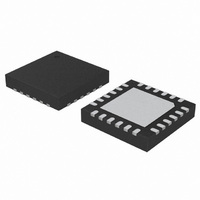
SI5356A-A-GM Silicon Laboratories Inc, SI5356A-A-GM Datasheet - Page 14

SI5356A-A-GM
Manufacturer Part Number
SI5356A-A-GM
Description
IC CLK GENERATOR 200MHZ 24-QFN
Manufacturer
Silicon Laboratories Inc
Datasheet
1.SI5356A-A-GM.pdf
(26 pages)
Specifications of SI5356A-A-GM
Package / Case
24-QFN
Pll
Yes
Input
CMOS, Crystal
Output
CMOS
Number Of Circuits
1
Ratio - Input:output
2:8
Differential - Input:output
No/No
Frequency - Max
200MHz
Divider/multiplier
Yes/No
Voltage - Supply
1.71 V ~ 3.63 V
Operating Temperature
-40°C ~ 85°C
Mounting Type
Surface Mount
Frequency-max
*
Max Input Freq
200 MHz
Supply Voltage (max)
3.3 V
Supply Voltage (min)
1.8 V
Max Output Freq
200 MHz
Mounting Style
SMD/SMT
Lead Free Status / RoHS Status
Lead free / RoHS Compliant
For Use With
336-1750 - EVALUATION BOARD FOR SI5356
Lead Free Status / Rohs Status
Lead free / RoHS Compliant
Other names
336-1749-5
Si5356
3.10. I
The Si5356 control interface is a 2-wire bus for
bidirectional communication. The bus consists of a
bidirectional serial data line (SDA) and a serial clock
input (SCL). The device operates as a slave device on
the 2-wire bus and is compatible with I
Both lines must be connected to the positive supply via
an external pull-up. Standard-Mode (100 kbps) and
Fast-Mode (400 kbps) operation and 7-bit addressing
are supported as specified in the I
standard. To accommodate multiple Si5356 devices on
the same I
The complete 7-bit I2C bus address for the device is
70h or 71h depending upon the state of the I2C_LSB
pin. In binary, this is written as 111 000[I2C_LSB]. See
14
S
2
C Interface
Slv Addr [6:0]
2
C bus, the Si5356 has pin 3 as I2C_LSB.
S
218
Slv Addr [6:0]
Write Data
0
S
7
1 – Read
0 – Write
A – Acknowledge (SDA LOW)
N – Not Acknowledge (SDA HIGH).
S – START condition
P – STOP condition
A
Figure 8. I
Slv Addr [6:0]
Reg Addr [7:0]
Required after the last data byte to signal the end of the read comand to the slave.
0
6
From master to slave
A
2
C-Bus Specification
Reg Addr [7:0]
2
5
2
C specifications.
C/SMBus-Compatible Command Format
0
Figure 7. Status Register
A
LOL
A
4
Two Command Read
Repeated Start Read
P
Reg Addr [7:0]
Preliminary Rev. 0.3
A
LOS
Clk
3
S
Write
S
Slv Addr [6:0] 1 A
XTAL
LOS
Slv Addr [6:0]
Figure 8 for the command format for both read and write
access.
Data is always sent MSB first. Table 7 includes the AC
and DC electrical parameters for the SCL and SDA I/
Os, respectively. The timing specifications and timing
diagram for the I
Specification
supported for compatibility with SMBus interfaces.
The I
The I
3.63 V
recommended by the I
2
A
From slave to master
Data [7:0]
2
2
C interface is 3.3 V tolerant.
C bus can be operated at a bus voltage of 1.71 to
1
and
SYS
1
Cal
0
A
standard.
should
A
Data [7:0]
Read Data
Optional
2
Data [7:0]
C bus can be found in the I
Data [7:0]
2
C-Bus Specification.
System Calibration
(Lock Acquisition)
Loss of Signal
XTAL Input
Loss of Signal
Clock Input
Loss of Lock
have
A
SDA
A
Optional
Data [7:0]
P
a
A
timeout
Optional
Data [7:0]
pullup
N P
resistor
N P
support
2
C-Bus
as
is


