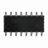
FS6377-01IG-XTD ON Semiconductor, FS6377-01IG-XTD Datasheet - Page 16

FS6377-01IG-XTD
Manufacturer Part Number
FS6377-01IG-XTD
Description
IC CLOCK GEN 3-PLL PROGR 16-SOIC
Manufacturer
ON Semiconductor
Type
PLL Clock Generatorr
Datasheet
1.FS6377-01G-XTD.pdf
(24 pages)
Specifications of FS6377-01IG-XTD
Pll
Yes
Input
Crystal
Output
CMOS
Number Of Circuits
1
Ratio - Input:output
1:4
Differential - Input:output
No/No
Frequency - Max
230MHz
Divider/multiplier
Yes/No
Voltage - Supply
3 V ~ 5.5 V
Operating Temperature
-40°C ~ 85°C
Mounting Type
Surface Mount
Package / Case
16-SOIC (3.9mm Width)
Frequency-max
230MHz
Number Of Elements
3
Pll Input Freq (min)
5MHz
Pll Input Freq (max)
27MHz
Operating Supply Voltage (typ)
3.3/5V
Operating Temp Range
-40C to 85C
Package Type
SOIC
Output Frequency Range
0.8 to 150MHz
Operating Supply Voltage (min)
3V
Operating Supply Voltage (max)
5.5V
Operating Temperature Classification
Industrial
Pin Count
16
Mounting Style
SMD/SMT
Number Of Outputs
1
Operating Temperature Range
0 C to + 70 C
Supply Current
43 mA
Lead Free Status / RoHS Status
Lead free / RoHS Compliant
Other names
766-1027
Available stocks
Company
Part Number
Manufacturer
Quantity
Price
Company:
Part Number:
FS6377-01IG-XTD
Manufacturer:
ON Semiconductor
Quantity:
135
Company:
Part Number:
FS6377-01IG-XTD
Manufacturer:
Exar
Quantity:
40
FS6377
Table 12: DC Electrical Specifications (continued)
Unless otherwise stated, V
nominal characterization data and are not currently production tested on any specific limits. Min. and max. characterization data are ± 3σ from typical. Negative currents
indicate current flows out of the device.
Mode and Frequency Select Inputs (ADDR, SEL_CD)
High-level input voltage
Low-level input voltage
High-level input current
Low-level input current (pull-up)
Crystal Oscillator Feedback (XIN)
Threshold bias voltage
High-level input current
Low-level input current
Crystal loading capacitance*
Input loading capacitance*
Crystal Oscillator Driver (XOUT)
High-level output source current
Low-level output sink current
Clock Outputs (CLK_A, CLK_B, CLK_C, CLK_D)
High-level output source current
Low-level output sink current
Output impedance
Tristate output current
Short circuit source current*
Short circuit sink current*
Voltage
(V)
0
0.2
0.5
0.7
1
1.2
1.5
1.7
2
2.2
2.5
2.7
3
3.5
4
4.5
5
5.5
Low Drive Current (mA)
DD
Min.
0
9
22
29
39
44
51
55
60
62
65
65
66
67
68
69
= 5.0V ± 10%, no load on any output, and ambient temperature range T
Typ.
0
11
25
34
46
52
61
66
73
77
81
83
85
87
88
89
91
Max.
0
12
29
40
55
64
76
83
92
97
104
108
112
117
119
120
121
123
V
V
I
I
V
I
I
C
C
I
I
I
I
Z
Z
I
I
I
IH
IL
IH
IL
OH
OL
OH
OL
Z
SCH
SCL
OH
OL
IH
IL
TH
L(xtal)
L(XIN)
Voltage
(V)
0
0.5
1
1.5
2
2.5
2.7
3
3.2
3.5
3.7
4
4.2
4.5
4.7
5
5.2
5.5
Figure 9: CLK_A, CLK_B, CLK_C, CLK_D Clock Outputs
High Drive Current (mA)
Rev. 4 | Page 16 of 24 | www.onsemi.com
V
V
V
V
V
V
V
V
V
As
connected to XIN and XOUT
As seen by an external clock driver on
XOUT; XIN unconnected
V
V
V
V
V
V
V
max.
V
DD
DD
DD
DD
DD
DD
DD
DD
DD
DD
DD
O
O
O
O
DD
DD
Min.
-87
-85
-83
-80
-74
-65
-61
-53
-48
-39
-32
-21
-13
0
= 2.4V
= 0.4V
= 0.5VDD; output driving high
= 0.5VDD; output driving low
= 5.5V
= 3.6V
= 5.5V
= 3.6V
= 5.5V
= 3.6V
= 5.5V
= 5.5V, oscillator powered down
= 5.5V
= V
= 5.5V, V
= V
= 5.5V, V
seen
(XIN)
O
= 5.5V; shorted for 30s, max.
Typ.
-112
-110
-108
-104
-97
-88
-84
-77
-71
-62
-55
-44
-36
-24
-15
0
= 5.5V, V
by
(XIN)
O
= 0V; shorted for 30s,
Max.
-150
-147
-144
-139
-131
-121
-116
-108
-102
-92
-85
-74
-65
-52
-43
-28
-11
0
= 0V, V
an
O
= 0V
external
O
= 5.5V
A
= 0°C to 70°C. Parameters denoted with an asterisk (*) represent
The data in this table represents nominal characterization data only.
crystal
V
V
SS
SS
2.4
2.0
-20
-25
-10
-10
10
-1
5
- 0.3
- 0.3
-125
-150
123
-36
2.9
1.7
-54
-21
54
18
36
21
23
29
27
V
V
DD
DD
-80
-75
-30
0.8
0.8
15
30
10
1
+0.3
+0.3
mA
mA
mA
mA
mA
mA
mA
µA
µA
µA
µA
µA
pF
pF
V
V
V
Ω


