ICS8761CYLF IDT, Integrated Device Technology Inc, ICS8761CYLF Datasheet
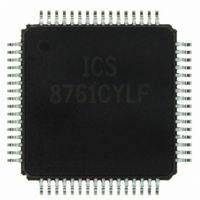
IC CLK GEN PCI/PCI-X 64-LQFP

ICS8761CYLF

Manufacturer Part Number
ICS8761CYLF
Description
IC CLK GEN PCI/PCI-X 64-LQFP
Manufacturer
IDT, Integrated Device Technology Inc
Series
HiPerClockS™r
Type
Clock Generatorr
Datasheet

Specifications of ICS8761CYLF

Pll
Yes with Bypass
Input
LVCMOS, LVTTL, Crystal
Output
LVCMOS, LVTTL
Number Of Circuits
1
Ratio - Input:output
2:16
Differential - Input:output
No/No
Frequency - Max
166.67MHz
Divider/multiplier
Yes/Yes
Voltage - Supply
3.135 V ~ 3.465 V
Operating Temperature
0°C ~ 85°C
Mounting Type
Surface Mount
Package / Case
64-LQFP
Frequency-max
167MHz
Lead Free Status / RoHS Status
Lead free / RoHS Compliant
Other names
800-1222
8761CYLF

Available stocks

Company
Part Number
Manufacturer
Quantity
Price
Part Number:
ICS8761CYLF
Manufacturer:
IDT
Quantity:
208
Part Number:
ICS8761CYLF
Manufacturer:
IDT, Integrated Device Technology Inc
Quantity:
10 000
Part Number:
ICS8761CYLFT
Manufacturer:
IDT, Integrated Device Technology Inc
Quantity:
10 000
FBDIV_SEL1
FBDIV_SEL0
B
8761CY
G
The ICS8761 is a low voltage, low skew PCI /
PCI-X Clock Generator. The ICS8761 has a selectable
REF_CLK or crystal input. The REF_CLK input accepts
LVCMOS or LVTTL input levels. The ICS8761 has a fully
intgrated PLL along with frequency configurable clock and
feedback outputs for multiplying and regenerating clocks with
“zero delay”. Using a 20MHz or 25MHz crystal or a 33.333MHz
or 66.666MHz reference frequency, the ICS8761 will
generate output frequencies of 33.333MHz, 66.666MHz,
100MHz and 133.333MHz simultaneously.
The low impedance LVCMOS/LVTTL outputs of the ICS8761
are designed to drive 50Ω series or parallel terminated
transmission lines.
XTAL_SEL
XTAL1
XTAL2
REF_CLK
D_SELA0
D_SELA1
D_SELB1
D_SELB0
D_SELC1
D_SELC0
D_SELD1
D_SELD0
PLL_SEL
LOCK
ENERAL
FB_IN
OEA
OEB
OEC
OED
MR
OSC
D
IAGRAM
D
0
1
ESCRIPTION
PLL
0
1
÷12
÷12
÷16
÷20
÷3
÷4
÷6
÷6
0 0
0 1
1 0
1 1
0 0
0 1
1 0
1 1
0 0
0 1
1 0
1 1
0 0
0 1
1 0
1 1
0 0
0 1
1 0
1 1
FB_OUT
QA0
QA1
QA2
QA3
QB0
QB1
QB2
QB3
QC0
QC1
QC2
QC3
QD0
QD1
QD2
QD3
www.idt.com
XTAL_SEL
REF_CLK
D_SELC0
D_SELC1
D_SELA0
D_SELA1
PLL_SEL
XTAL1
XTAL2
GND
OEC
OEA
GND
V
1
V
V
DDA
DD
DD
P
F
• Fully integrated PLL
• Seventeen LVCMOS/LVTTL outputs,
• Selectable crystal oscillator interface or
• Maximum output frequency: 166.67MHz
• Maximum crystal input frequency: 38MHz
• Maximum REF_CLK input frequency: 83.33MHz
• Individual banks with selectable output dividers for
• Separate feedback control for generating PCI / PCI-X
• Cycle-to-cycle jitter: 70ps (maximum)
• Period jitter, RMS: 17ps (maximum)
• Output skew: 230ps (maximum)
• Bank skew: 40ps (maximum)
• Static phase offset: 0 ± 150ps (maximum)
• Full 3.3V or 3.3V core, 2.5V multiple output supply modes
• 0°C to 85°C ambient operating temperature
• Available in both standard and lead-free RoHS-compliant
15Ω typical output impedance
LVCMOS/LVTTL REF_CLK
generating 33.333MHz, 66.66MHz, 100MHz and
133.333MHz simultaneously
frequencies from a 20MHz or 25MHz crystal or 33.333MHz
or 66.666MHz reference frequency
packages
EATURES
IN
1
2
3
4
5
6
7
8
9
10
11
12
13
14
15
16
17 18 19 20 21 22 23 24 25 26 27 28 29 30 31 32
64 63 62 61 60 59 58 57 56 55 54 53 52 51 50 49
A
10mm x 10mm x 1.4mm package body
SSIGNMENT
PCI / PCI-X C
64-Lead LQFP
ICS8761
Y package
Top View
L
OW
V
OLTAGE
LOCK
ICS8761
, L
G
REV. E JULY 26, 2010
OW
ENERATOR
48
47
46
45
44
43
42
41
40
39
38
37
36
35
34
33
S
GND
FB_OUT
V
FB_IN
V
FBDIV_SEL0
FBDIV_SEL1
MR
V
D_SELD0
D_SELD1
OED
OEB
D_SELB0
D_SELB1
GND
DDOFB
DD
DD
KEW
,

Related parts for ICS8761CYLF

ICS8761CYLF Summary of contents

Page 1

G D ENERAL ESCRIPTION The ICS8761 is a low voltage, low skew PCI / PCI-X Clock Generator. The ICS8761 has a selectable REF_CLK or crystal input. The REF_CLK input accepts LVCMOS or LVTTL input levels. The ICS8761 has a fully ...

Page 2

ABLE IN ESCRIPTIONS ...

Page 3

...

Page 4

T 3D ABLE ONTROL UNCTION ABLE ...

Page 5

BSOLUTE AXIMUM ATINGS Supply Voltage Inputs, V -0. Outputs, V -0. Package Thermal Impedance, θ JA Storage Temperature, T -65°C to 150°C STG T 4A ...

Page 6

T 4C. LVCMOS/LVTTL DC C ABLE HARACTERISTICS ...

Page 7

T 7A ABLE HARACTERISTICS ...

Page 8

P ARAMETER 1.65V± DDA, DDOx LVCMOS GND -1.165V±5% 3. UTPUT OAD EST IRCUIT V DDOX DDOX sk( UTPUT KEW V V DDOX DDOX ...

Page 9

OWER UPPLY ILTERING ECHNIQUES As in any high speed analog circuitry, the power supply pins are vulnerable to random noise. The ICS8761 provides separate power supplies to isolate any high switching noise from the outputs to ...

Page 10

ECOMMENDATIONS FOR NUSED I : NPUTS RYSTAL NPUT For applications not requiring the use of the crystal oscillator input, both XTAL_IN and XTAL_OUT can be left floating. Though not required, but for additional protection, ...

Page 11

S E CHEMATIC XAMPLE Figure 3 shows a schematic example of the ICS8761. In this example, the input is driven by an ICS LVHSTL driver. The decoupling capacitors should be physically located near the VDD ...

Page 12

ABLE VS IR LOW ABLE FOR JA Single-Layer PCB, JEDEC Standard Test Boards Multi-Layer PCB, JEDEC Standard Test Boards NOTE: Most modern PCB designs use multi-layered boards. The data in the second row ...

Page 13

ACKAGE UTLINE UFFIX FOR ABLE ...

Page 14

T 10 ABLE RDERING NFORMATION ...

Page 15

...

Page 16

We’ve Got Your Timing Solution. 6024 Silver Creek Valley Road San Jose, CA 95138 © 2010 Integrated Device Technology, Inc. All rights reserved. Product specifications subject to change without notice. IDT, the IDT logo, ICS and HiPerClockS are trademarks of ...

Related keywords