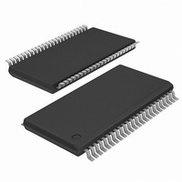
IDT5T915PAGI IDT, Integrated Device Technology Inc, IDT5T915PAGI Datasheet - Page 12

IDT5T915PAGI
Manufacturer Part Number
IDT5T915PAGI
Description
IC CLK BUFFER 1:5 DIFF 48-TSSOP
Manufacturer
IDT, Integrated Device Technology Inc
Type
Fanout Buffer (Distribution)r
Datasheet
1.IDT5T915PAGI8.pdf
(19 pages)
Specifications of IDT5T915PAGI
Number Of Circuits
1
Ratio - Input:output
1:5
Differential - Input:output
Yes/Yes
Input
eHSTL, HSTL, LVPECL, LVTTL
Output
eHSTL, HSTL, LVTTL
Frequency - Max
250MHz
Voltage - Supply
2.4 V ~ 2.6 V
Operating Temperature
-40°C ~ 85°C
Mounting Type
Surface Mount
Package / Case
48-TSSOP
Frequency-max
250MHz
Number Of Outputs
10
Operating Supply Voltage (max)
2.6V
Operating Temp Range
-40C to 85C
Propagation Delay Time
3.5ns
Operating Supply Voltage (min)
2.4V
Mounting
Surface Mount
Pin Count
48
Operating Supply Voltage (typ)
2.5V
Package Type
TSSOP
Quiescent Current
30mA
Operating Temperature Classification
Industrial
Lead Free Status / RoHS Status
Lead free / RoHS Compliant
Other names
5T915PAGI
NOTES:
1. Skew measured between all outputs or output pairs under identical input and output interfaces, transitions and load conditions on any one device. For single ended and differential
2. For operating with either 1.8V or 2.5V LVTTL output interfaces with both true and complementary outputs enabled. Inverting skew is the skew between true and complementary
3. Skew measured is the difference between propagation delay times t
4. Skew measured is the magnitude of the difference in propagation times between any outputs or output pairs of two devices, given identical transitions and load conditions at identical
5. Guaranteed by design.
AC ELECTRICAL CHARACTERISTICS OVER OPERATING RANGE
Skew Parameters
Propagation Delay
Output Gate Enable/Disable Delay
IDT5T915
2.5V DIFFERENTIAL 1:5 CLOCK BUFFER TERABUFFER
LVTTL outputs, this measurement is made when each output voltage passes through V
outputs and the complementary outputs are compared only with other complementary outputs. For differential HSTL outputs, the measurement takes place at the crossing point
of the true and complementary signals.
outputs switching in opposite directions under identical input and output interfaces, transitions and load conditions on any one device.
on any one device. For single ended and differential LVTTL outputs, this measurement is made when each output voltage passes through V
to both true and complementary signals. For differential HSTL outputs, the measurement takes place at the crossing point of the true and complementary signals.
V
Symbol
t
DD
t
SK
t
t
SK
SK
SK
V
t
t
t
t
PGE
PGD
PLH
PHL
/V
(
t
t
f
(
OX
R
F
O
(
INV
(
PP
O
P
DDQ
)
)
)
)
levels and temperature.
Parameter
Same Device Output Pin-to-Pin Skew
Inverting Skew
Pulse Skew
Part-to-Part Skew
HSTL and eHSTL Differential True and Complementary Output Crossing Voltage Level
Propagation Delay A to Qn/Qn
Output Rise Time (20% to 80%)
Output Fall Time (20% to 80%)
Frequency Range (HSTL/eHSTL outputs)
Frequency Range (2.5V/1.8V LVTTL outputs)
Output Gate Enable to Qn/Qn
Output Gate Enable to Qn/Qn Driven to GL Designated Level
(3)
(2)
(4)
PHL
(1)
and t
PLH
Single-Ended and Differential Modes
Single-Ended in Differential Mode (DSE)
Single-Ended and Differential Modes
Single-Ended in Differential Mode (DSE)
Single-Ended and Differential Modes
Single-Ended in Differential Mode (DSE)
Single-Ended and Differential Modes
Single-Ended in Differential Mode (DSE)
2.5V / 1.8V LVTTL Outputs
HSTL / eHSTL Outputs
2.5V / 1.8V LVTTL Outputs
HSTL / eHSTL Outputs
2.5V / 1.8V LVTTL Outputs
HSTL / eHSTL Outputs
of any output or output pair under identical input and output interfaces, transitions and load conditions
12
DDQ
/2. For differential LVTTL outputs, the true outputs are compared only with other true
V
DDQ
INDUSTRIAL TEMPERATURE RANGE
Min.
350
350
350
350
—
—
—
—
—
—
—
—
/2 - 200
—
—
—
—
—
—
V
(5)
Typ.
DDQ
300
300
300
DDQ
—
25
—
—
—
—
—
—
—
—
—
—
—
—
—
/2
/2. The measurement applies
V
DDQ
1050
1350
1050
1350
Max
300
300
300
250
200
/2 + 200
2.5
3.5
25
—
—
—
—
2
3
MHz
Unit
mV
ps
ps
ps
ps
ns
ps
ps
ns
ns


