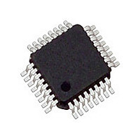
ICS8312AYILF IDT, Integrated Device Technology Inc, ICS8312AYILF Datasheet - Page 10

ICS8312AYILF
Manufacturer Part Number
ICS8312AYILF
Description
IC FANOUT BUFFER 1:12 32-LQFP
Manufacturer
IDT, Integrated Device Technology Inc
Series
HiPerClockS™r
Type
Fanout Buffer (Distribution)r
Datasheet
1.ICS8312AYILFT.pdf
(18 pages)
Specifications of ICS8312AYILF
Number Of Circuits
1
Ratio - Input:output
1:12
Differential - Input:output
No/No
Input
LVCMOS, LVTTL
Output
LVCMOS, LVTTL
Frequency - Max
250MHz
Voltage - Supply
1.6 V ~ 3.465 V
Operating Temperature
-40°C ~ 85°C
Mounting Type
Surface Mount
Package / Case
32-LQFP
Frequency-max
250MHz
Number Of Outputs
12
Operating Supply Voltage (max)
3.465V
Operating Temp Range
-40C to 85C
Propagation Delay Time
4.9ns
Operating Supply Voltage (min)
1.6V
Mounting
Surface Mount
Pin Count
32
Operating Supply Voltage (typ)
1.8/2.5/3.3V
Package Type
TQFP
Duty Cycle
55%
Operating Temperature Classification
Industrial
Lead Free Status / RoHS Status
Lead free / RoHS Compliant
Other names
8312AYILF
Available stocks
Company
Part Number
Manufacturer
Quantity
Price
Company:
Part Number:
ICS8312AYILF
Manufacturer:
ST
Quantity:
220
Company:
Part Number:
ICS8312AYILF
Manufacturer:
IDT, Integrated Device Technology Inc
Quantity:
10 000
Company:
Part Number:
ICS8312AYILFT
Manufacturer:
IDT, Integrated Device Technology Inc
Quantity:
10 000
Additive Phase Jitter
The spectral purity in a band at a specific offset from the
fundamental compared to the power of the fundamental is called
the dBc Phase Noise. This value is normally expressed using a
Phase noise plot and is most often the specified plot in many
applications. Phase noise is defined as the ratio of the noise power
present in a 1Hz band at a specified offset from the fundamental
frequency to the power value of the fundamental. This ratio is
expressed in decibels (dBm) or a ratio of the power in the 1Hz band
As with most timing specifications, phase noise measurements
has issues relating to the limitations of the equipment. Often the
noise floor of the equipment is higher than the noise floor of the
IDT™ / ICS™ LVCMOS/LVTTL FANOUT BUFFER
ICS8312I
LOW SKEW, 1-TO-12 LVCMOS/LVTTL FANOUT BUFFER
Offset from Carrier Frequency (Hz)
10
to the power in the fundamental. When the required offset is
specified, the phase noise is called a dBc value, which simply
means dBm at a specified offset from the fundamental. By
investigating jitter in the frequency domain, we get a better
understanding of its effects on the desired application over the
entire time record of the signal. It is mathematically possible to
calculate an expected bit error rate given a phase noise plot.
device. This is illustrated above. The device meets the noise floor
of what is shown, but can actually be lower. The phase noise is
dependant on the input source and measurement equipment.
Additive Phase Jitter, 3.3V @ 100MHz
12kHz to 20MHz = 0.037ps (typical)
ICS8312AYI REV. B JUNE 24, 2008


