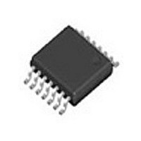
ICS8535AGI-21LFT IDT, Integrated Device Technology Inc, ICS8535AGI-21LFT Datasheet - Page 3

ICS8535AGI-21LFT
Manufacturer Part Number
ICS8535AGI-21LFT
Description
IC CLOCK GEN 1-2 LVPECL 14-TSSOP
Manufacturer
IDT, Integrated Device Technology Inc
Type
Fanout Buffer (Distribution), Multiplexerr
Series
HiPerClockS™r
Datasheet
1.ICS8535AGI-21LFT.pdf
(14 pages)
Specifications of ICS8535AGI-21LFT
Number Of Circuits
1
Ratio - Input:output
2:2
Differential - Input:output
No/Yes
Input
LVCMOS, LVTTL
Output
LVPECL
Frequency - Max
266MHz
Voltage - Supply
3.135 V ~ 3.465 V
Operating Temperature
-40°C ~ 85°C
Mounting Type
Surface Mount
Package / Case
14-TSSOP
Frequency-max
266MHz
Number Of Clock Inputs
2
Mode Of Operation
Single-Ended
Output Frequency
266MHz
Output Logic Level
LVPECL
Operating Supply Voltage (min)
3.135V
Operating Supply Voltage (typ)
3.3V
Operating Supply Voltage (max)
3.465V
Package Type
TSSOP
Operating Temp Range
-40C to 85C
Operating Temperature Classification
Industrial
Signal Type
LVCMOS/LVTTL
Mounting
Surface Mount
Pin Count
14
Lead Free Status / RoHS Status
Lead free / RoHS Compliant
Other names
8535AGI-21LFT
Function Tables
Table 3A. Control Input Function Table
After CLK_EN switches, the clock outputs are disabled or enabled following a rising and falling input clock edge as shown in Figure 1.
In the active mode, the state of the outputs are a function of the CLK0 and CLK1 inputs as described in Table 3B.
Figure 1. CLK_EN Timing Diagram
Table 3B. Clock Input Function Table
IDT™ / ICS™ 3.3V LVPECL FANOUT BUFFER
CLK0, CLK1
ICS8535I-21
LOW SKEW, 1-TO-2 LVCMOS/LVTTL-TO-3.3V LVPECL FANOUT BUFFER
nQ0, nQ1
CLK0 or CLK1
CLK_EN
Q0, Q1
CLK_EN
Inputs
Inputs
0
0
1
1
0
1
Q0, Q1
CLK_SEL
HIGH
LOW
0
1
0
1
Disabled
Outputs
nQ0, nQ1
HIGH
LOW
Selected Source
CLK0
CLK1
CLK0
CLK1
3
Disabled; Low
Disabled; Low
Enabled
Enabled
Q0, Q1
Outputs
Enabled
ICS8535AGI-21 REV. A NOVEMBER 24, 2008
Disabled; High
Disabled; High
nQ0, nQ1
Enabled
Enabled


