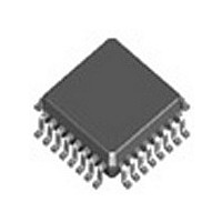
MPC9446AC IDT, Integrated Device Technology Inc, MPC9446AC Datasheet - Page 6

MPC9446AC
Manufacturer Part Number
MPC9446AC
Description
IC CLK FANOUT BUFFER 32-LQFP
Manufacturer
IDT, Integrated Device Technology Inc
Type
Fanout Buffer (Distribution), Divider, Multiplexer , PLLr
Datasheet
1.MPC9446FA.pdf
(11 pages)
Specifications of MPC9446AC
Number Of Circuits
1
Ratio - Input:output
2:10
Differential - Input:output
No/No
Input
LVCMOS
Output
LVCMOS
Frequency - Max
250MHz
Voltage - Supply
2.375 V ~ 3.465 V
Operating Temperature
-40°C ~ 85°C
Mounting Type
Surface Mount
Package / Case
32-LQFP
Frequency-max
250MHz
Number Of Clock Inputs
2
Mode Of Operation
Single-Ended
Output Frequency
250MHz
Output Logic Level
LVCMOS
Operating Supply Voltage (min)
2.375V
Operating Supply Voltage (typ)
2.5/3.3V
Operating Supply Voltage (max)
3.465V
Package Type
TQFP
Operating Temp Range
-40C to 85C
Operating Temperature Classification
Industrial
Signal Type
LVCMOS
Mounting
Surface Mount
Pin Count
32
Quiescent Current
2mA
Lead Free Status / RoHS Status
Lead free / RoHS Compliant
Available stocks
Company
Part Number
Manufacturer
Quantity
Price
Company:
Part Number:
MPC9446AC
Manufacturer:
Freescal
Quantity:
490
Company:
Part Number:
MPC9446AC
Manufacturer:
IDT, Integrated Device Technology Inc
Quantity:
10 000
Part Number:
MPC9446AC
Manufacturer:
IDT
Quantity:
20 000
Company:
Part Number:
MPC9446ACR2
Manufacturer:
IDT
Quantity:
392
Company:
Part Number:
MPC9446ACR2
Manufacturer:
IDT
Quantity:
402
Company:
Part Number:
MPC9446ACR2
Manufacturer:
IDT, Integrated Device Technology Inc
Quantity:
10 000
Part Number:
MPC9446ACR2
Manufacturer:
IDT
Quantity:
20 000
Company:
Part Number:
MPC9446ACZ
Manufacturer:
FREESCA
Quantity:
2
IDT™ / ICS™ LVCMOS CLOCK FANOUT BUFFER
MPC9446
3.3V AND 2.5V LVCMOS CLOCK FANOUT BUFFER
Driving Transmission Lines
speed signals in a terminated transmission line environment.
To provide the optimum flexibility to the user, the output
drivers were designed to exhibit the lowest impedance
possible. With an output impedance of less than 20 Ω, the
drivers can drive either parallel or series terminated
transmission lines. For more information on transmission
lines the reader is referred to Freescale application note
AN1091. In most high performance clock networks,
point-to-point distribution of signals is the method of choice.
In a point-to-point scheme, either series terminated or parallel
terminated transmission lines can be used. The parallel
technique terminates the signal at the end of the line with a
50 Ω resistance to V
thus, only a single terminated line can be driven by each
output of the MPC9446 clock driver. For the series terminated
case, however, there is no DC current draw; thus, the outputs
can drive multiple series terminated lines.
an output driving a single series terminated line versus two
series terminated lines in parallel. When taken to its extreme,
the fanout of the MPC9446 clock driver is effectively doubled
due to its capability to drive multiple lines.
results of an output driving a single line versus two lines. In
both cases, the drive capability of the MPC9446 output buffer
is more than sufficient to drive 50 Ω transmission lines on the
incident edge. Note from the delay measurements in the
simulations, a delta of only 43 ps exists between the two
differently loaded outputs. This suggests that the dual line
driving need not be used exclusively to maintain the tight
output-to-output skew of the MPC9446. The output waveform
in
by the impedance mismatch seen looking into the driver. The
parallel combination of the 36 Ω series resistor plus the
output impedance does not match the parallel combination of
IN
IN
Figure 4
The MPC9446 clock driver was designed to drive high-
This technique draws a fairly high level of DC current, and
The waveform plots in
Figure 3. Single versus Dual Transmission Lines
MPC9446
MPC9446
Output
Output
Buffer
14Ω
Buffer
14Ω
shows a step in the waveform. This step is caused
CC
÷2.
R
R
R
S
S
S
Figure 4
= 36Ω
= 36Ω
= 36Ω
show the simulation
Z
Z
Z
O
O
O
= 50Ω
= 50Ω
= 50Ω
Figure 3
APPLICATIONS INFORMATION
illustrates
OutA
OutB0
OutB1
the line impedances. The voltage wave launched down the
two lines will equal:
unity reflection coefficient, to 2.5 V. It will then increment
towards the quiescent 3.0 V in steps separated by one round
trip delay (in this case 4.0 ns).
cause any false clock triggering; however, designers may be
uncomfortable with unwanted reflections on the line. To better
match the impedances when driving multiple lines, the
situation in
terminating resistors are reduced such that when the parallel
combination is added to the output buffer impedance, the line
impedance is perfectly matched.
At the load end, the voltage will double, due to the near
Since this step is well above the threshold region, it will not
3.0
2.5
2.0
1.5
1.0
0.5
0
Figure 5. Optimized Dual Line Termination
Figure 4. Single versus Dual Waveforms
14 Ω + 22 Ω || 22 Ω = 50 Ω || 50 Ω
t
Figure 5
MPC9446
D
2
Output
14Ω
Buffer
= 3.8956
OutA
In
V
Z
R
R
V
0
L
L
S
0
= V
= 50 Ω || 50 Ω
= 36 Ω || 36 Ω
= 14 Ω
= 3.0 (25 ÷ (18 + 14 + 25)
= 1.31 V
4
should be used. In this case, the series
25 Ω = 25 Ω
S
(Z
0
R
R
6
÷ (R
S
S
= 22Ω
= 22Ω
Time (ns)
6MPC9446 REV 4 NOVEMBER 28, 2007)
t
S
D
= 3.9386
+ R
OutB
8
0
Z
Z
+ Z
O
O
10
= 50Ω
= 50Ω
0
))
12
14


