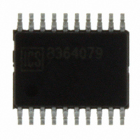
ICS85356AGILF IDT, Integrated Device Technology Inc, ICS85356AGILF Datasheet - Page 4

ICS85356AGILF
Manufacturer Part Number
ICS85356AGILF
Description
IC CLK MUX 2:1 DIFF HS 20-TSSOP
Manufacturer
IDT, Integrated Device Technology Inc
Series
HiPerClockS™r
Type
Multiplexerr
Datasheet
1.ICS85356AGILF.pdf
(15 pages)
Specifications of ICS85356AGILF
Number Of Circuits
2
Ratio - Input:output
2:1
Differential - Input:output
Yes/Yes
Input
HCSL, LVDS, LVHSTL, LVPECL, SSTL
Output
LVPECL
Frequency - Max
900MHz
Voltage - Supply
3 V ~ 3.6 V
Operating Temperature
-40°C ~ 85°C
Mounting Type
Surface Mount
Package / Case
20-TSSOP
Frequency-max
900MHz
Number Of Clock Inputs
4/2
Mode Of Operation
Differential
Output Frequency
900MHz
Output Logic Level
ECL/LVPECL
Operating Supply Voltage (min)
-3/3V
Operating Supply Voltage (typ)
-3.3/3.3V
Operating Supply Voltage (max)
-3.8/3.6V
Package Type
TSSOP
Operating Temp Range
-40C to 85C
Operating Temperature Classification
Industrial
Mounting
Surface Mount
Pin Count
20
Lead Free Status / RoHS Status
Lead free / RoHS Compliant
Other names
800-1175
800-1175-5
800-1175
85356AGILF
800-1175-5
800-1175
85356AGILF
ICS85356I Data Sheet
Table 4C. Differential DC Characteristics, V
NOTE 1: VIL should not be less than -0.3V
NOTE 2: Common mode voltage is defined as V
Table 4D. LVPECL DC Characteristics, V
NOTE 1: Outputs termination with 50Ω to V
AC Electrical Characteristics
Table 5. AC Characteristics, V
NOTE: Electrical parameters are guaranteed over the specified ambient operating temperature range, which is established when the device is
mounted in a test socket with maintained transverse airflow greater than 500 lfpm. The device will meet specifications after thermal equilibrium
has been reached under these conditions
NOTE: All parameters measured at ƒ ≤ 622MHz, unless otherwise noted.
NOTE: This part does not add measurable jitter.
NOTE 1: Measured from the differential input crossing point to the differential output crossing point.
NOTE 2: Defined as skew between outputs at the same supply voltage and with equal load conditions.
Measured at the output differential cross points.
NOTE 3: This parameter is defined according with JEDEC Standard 65.
ICS85356AMI REVISION B MAY 10, 2010
Symbol
I
I
V
V
Symbol
V
V
V
Symbol
f
t
tsk(o)
t
t
IH
IL
MAX
PD
R
ODC
OH
OL
PP
CMR
SWING
/ t
F
Parameter
Input
High Current
Input
Low Current
Peak-to-Peak Voltage; NOTE 1
Common Mode Range; NOTE 1, 2
Parameter
Output High Voltage; NOTE 1
Output Low Voltage; NOTE 1
Peak-to-Peak Output Voltage Swing
Parameter
Output Frequency
Propagation Delay; NOTE 1
Output Skew; NOTE 2, 3
Output Rise/Fall Time
Output Duty Cycle Skew
CLK0A, CLK0B,
CLK1A, CLK1B
nCLK0A, nCLK0B,
nCLK1A, nCLK1B
CLK0A, CLK0B,
CLK1A, CLK1B
nCLK0A, nCLK0B,
nCLK1A, nCLK1B
CC
= 3.3V±0.3V; V
CC
– 2V.
CC
IH
.
= 3.3V±0.3V; V
CC
= 3.3V±0.3V; V
EE
Test Conditions
V
V
ƒ ≤ 900MHz
= 0V, T
20% to 80%
CC
CC
V
V
Test Conditions
Test Conditions
CC
CC
= 3.6V, V
= 3.6V, V
= V
= V
A
EE
IN
IN
= -40°C to 85°C
4
= 3.6V
= 3.6V
= 0V, T
EE
IN
IN
= 0V, T
= 0V
= 0V
A
= -40°C to 85°C
A
2:1, DIFFERENTIAL-TO-3.3V LVPECL/ECL CLOCK MULTIPLEXER
= -40°C to 85°C
Minimum
Minimum
V
V
Minimum
V
CC
CC
0.85
200
EE
0.6
-150
0.15
– 1.4
– 2.0
-5
+ 0.5
Typical
Typical
1.15
Typical
900
75
©2010 Integrated Device Technology, Inc.
Maximum
Maximum
V
V
V
Maximum
CC
CC
CC
1.45
150
580
100
1.0
150
1.0
– 0.9
– 1.7
– 0.85
5
Units
Units
MHz
Units
ns
ps
ps
ps
µA
µA
µA
µA
V
V
V
V
V


