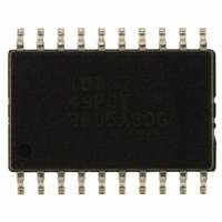
IDT49FCT3805ASOG IDT, Integrated Device Technology Inc, IDT49FCT3805ASOG Datasheet - Page 2

IDT49FCT3805ASOG
Manufacturer Part Number
IDT49FCT3805ASOG
Description
IC CLK BUFFER/DVR 1:5 20SOIC
Manufacturer
IDT, Integrated Device Technology Inc
Series
49FCTr
Type
Fanout Buffer (Distribution)r
Datasheet
1.IDT49FCT3805AQG8.pdf
(7 pages)
Specifications of IDT49FCT3805ASOG
Number Of Circuits
2
Ratio - Input:output
1:5
Differential - Input:output
No/No
Input
LVTTL
Output
CMOS
Frequency - Max
166MHz
Voltage - Supply
3 V ~ 3.6 V
Operating Temperature
0°C ~ 70°C
Mounting Type
Surface Mount
Package / Case
20-SOIC
Frequency-max
166MHz
Number Of Outputs
10
Operating Supply Voltage (max)
3.6V
Operating Temp Range
0C to 70C
Propagation Delay Time
5ns
Operating Supply Voltage (min)
3V
Mounting
Surface Mount
Pin Count
20
Operating Supply Voltage (typ)
3.3V
Package Type
SOIC
Quiescent Current
10uA
Operating Temperature Classification
Commercial
Lead Free Status / RoHS Status
Lead free / RoHS Compliant
Other names
49FCT3805ASOG
800-1343
800-1343-5
800-1343
800-1343
800-1343-5
800-1343
Available stocks
Company
Part Number
Manufacturer
Quantity
Price
Company:
Part Number:
IDT49FCT3805ASOG
Manufacturer:
IDT
Quantity:
677
Part Number:
IDT49FCT3805ASOG
Manufacturer:
IDT
Quantity:
20 000
Company:
Part Number:
IDT49FCT3805ASOG8
Manufacturer:
IDT
Quantity:
6 778
ABSOLUTE MAXIMUM RATINGS
NOTES:
1. Stresses greater than those listed under ABSOLUTE MAXIMUM RATINGS may cause
2. V
3. Input terminals.
4. Outputs and I/O terminals.
CAPACITANCE (T
NOTE:
1. This parameter is measured at characterization but not tested.
IDT49FCT3805/A
3.3V CMOS BUFFER/CLOCK DRIVER
Symbol
Symbol
V
V
V
C
TERM (2)
TERM (3)
TERM (4)
T
permanent damage to the device. This is a stress rating only and functional operation
of the device at these or any other conditions above those indicated in the operational
sections of this specification is not implied. Exposure to absolute maximum rating
conditions for extended periods may affect reliability.
C
I
OUT
OUT
STG
CC
IN
terminals.
Description
Terminal Voltage with Respect to GND
Terminal Voltage with Respect to GND
Terminal Voltage with Respect to GND
Storage Temperature
DC Output Current
Parameter
Input Capacitance
Output Capacitance
(1)
A
= +25
Conditions
V
V
OUT
IN
= 0V
= 0V
O
C, f = 1.0MHz)
Typ.
4.5
5.5
–0.5 to V
–0.5 to +4.6
–65 to +150
–60 to +60
–0.5 to +7
Max
CC
Max.
(1)
6
8
+0.5
Unit
pF
pF
Unit
mA
°C
V
V
V
2
PIN DESCRIPTION
FUNCTION TABLE
NOTE:
1. H = HIGH
L = LOW
Z = High-Impedance
OE
Pin Names
OAn, OBn
OE
IN
A
MON
H
H
, OE
COMMERCIAL AND INDUSTRIAL TEMPERATURE RANGE
A
L
L
A
, IN
, OE
B
B
B
Inputs
3-State Output Enable Inputs (Active LOW)
Clock Inputs
Clock Outputs
Monitor Output
IN
A
H
H
, IN
L
L
B
(1)
Description
OAn, OBn
H
L
Z
Z
Outputs
MON
H
H
L
L


