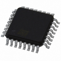
STLVD111BFR STMicroelectronics, STLVD111BFR Datasheet - Page 8

STLVD111BFR
Manufacturer Part Number
STLVD111BFR
Description
IC CLOCK DRVR DIFF LVDS 32-TQFP
Manufacturer
STMicroelectronics
Type
Fanout Buffer (Distribution), Multiplexerr
Datasheet
1.STLVD111BFR.pdf
(19 pages)
Specifications of STLVD111BFR
Number Of Circuits
1
Ratio - Input:output
1:10
Differential - Input:output
Yes/Yes
Input
LVDS
Output
LVDS
Frequency - Max
900MHz
Voltage - Supply
2.375 V ~ 2.625 V
Operating Temperature
-40°C ~ 85°C
Mounting Type
Surface Mount
Package / Case
32-TQFP, 32-VQFP
Frequency-max
900MHz
Lead Free Status / RoHS Status
Contains lead / RoHS non-compliant
Other names
497-2146-2
Available stocks
Company
Part Number
Manufacturer
Quantity
Price
Company:
Part Number:
STLVD111BFR
Manufacturer:
AD
Quantity:
204
Company:
Part Number:
STLVD111BFR
Manufacturer:
STMicroelectronics
Quantity:
10 000
Part Number:
STLVD111BFR
Manufacturer:
ST
Quantity:
20 000
4
4.1
4.2
Table 10.
Table 11.
Table 12.
8/19
CLK_SEL
BIT#10
EN
H
H
L
L
L
Specification of control register
The STLVD111 is provided with a 11 bit shift register with a Serial In and a Control Register.
The purpose is to enable or power of each output clock channel and to select the clock
input. The STLVD111 provides two working modality:
Programmed mode (EN=1)
The shift register have a serial input to load the working configuration. Once the
configuration is loaded with 11 clock pulse, another clock pulse load the configuration into
the control register. The first bit on the serial input line enables the outputs Q9 and Q9, the
second bit enables the outputs Q8 and Q8 and so on. The last bit is the clock selection bit.
To restart the configuration of the shift register a reset of the state machine must be done
with a clock pulse on CK and the EN set to Low. The control register shift register can be
configured on time after each reset.
Standard mode (EN=0)
In Standard Mode the STLVD111 isn’t programmable, all the clock outputs are enabled. The
LVDS clock input is selected from Clock 0 or Clock 1 with the SI pin as shown in the Truth
Table below.
Truth table of state machine inputs
Serial input sequence
Truth table of the control register
BIT#9
BIT#10
Q0
H
X
L
SI
H
H
X
L
L
BIT#8
Q1
BIT#7
Q2
CK
X
X
BIT#6
Q3
All output enabled, Clock 0 selected, control register disabled
All output enabled, Clock 1 selected, control register disabled
First stage stores "L", other stages store the data of previous stage
First stage stores "H", other stages store the data of previous stage
Reset of the state machine, shift register and control register
BIT#(0-9)
BIT#5
H
H
L
Q4
BIT#4
Q5
BIT#3
Output
Q6
Qn Output Disabled
BIT#2
Q7
Qn(0-9)
Clock 0
Clock 1
BIT#1
Q8
BIT#0
Q9


