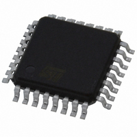
STLVD111BFR STMicroelectronics, STLVD111BFR Datasheet - Page 7

STLVD111BFR
Manufacturer Part Number
STLVD111BFR
Description
IC CLOCK DRVR DIFF LVDS 32-TQFP
Manufacturer
STMicroelectronics
Type
Fanout Buffer (Distribution), Multiplexerr
Datasheet
1.STLVD111BFR.pdf
(19 pages)
Specifications of STLVD111BFR
Number Of Circuits
1
Ratio - Input:output
1:10
Differential - Input:output
Yes/Yes
Input
LVDS
Output
LVDS
Frequency - Max
900MHz
Voltage - Supply
2.375 V ~ 2.625 V
Operating Temperature
-40°C ~ 85°C
Mounting Type
Surface Mount
Package / Case
32-TQFP, 32-VQFP
Frequency-max
900MHz
Lead Free Status / RoHS Status
Contains lead / RoHS non-compliant
Other names
497-2146-2
Available stocks
Company
Part Number
Manufacturer
Quantity
Price
Company:
Part Number:
STLVD111BFR
Manufacturer:
AD
Quantity:
204
Company:
Part Number:
STLVD111BFR
Manufacturer:
STMicroelectronics
Quantity:
10 000
Part Number:
STLVD111BFR
Manufacturer:
ST
Quantity:
20 000
Table 7.
Note:
Table 8.
Table 9.
Symbol
t
t
Symbol
PHL,
Symbol
TLH,
C
t
I
V
SKEW
CCD
C
V
f
f
V
t
MAX
MAX
OUT
rem
I
t
BB
t
IH
t
IN
IL
W
I
s
h
t
t
THL
PLH
1
2
Output reference voltage
Power supply current
Input capacitance
Output capacitance
Logic input high threshold
Logic input low threshold
Logic input current
LVDS timing characteristics (T
specified)
Transition time
Propagation delay time
Maximum input frequency
Bank skew
Part to part skew
Pulse skew
Control register timing characteristics (T
otherwise specified)
Maximum frequency of shift register
Clock to SI setup time
Clock to SI hold time
Enable to clock removal time
Minimum clock pulse width
Driver electrical characteristics (T
specified
All currents into device pins are positive; all currents out of device pins are negative. All
voltages are referenced to device ground unless otherwise specified
All typical values are given for V
Parameter
Parameter
Note:
Parameter
1, 2)
R
Figure
(Figure
(Figure
(Figure
(Figure
L
= 100 Ω , C
All driver enabled and loaded
V
V
V
V
V
CC
I
CC
CC
CC
CC
= 0V to V
(Figure
(Figure
(Figure
(Figure
(Figure
A
7.,
7.,
3.)
4.)
5.)
= 2.5 V
= 2.5 V
= 2.5 V
= 2.5 V, V
Test condition
= 2.5V and T
= -40 to 85 °C, V
A
Figure
Figure
Test condition
= -40 to 85 °C, V
Test condition
L
9.)
9.)
9.)
9.)
9.)
= 5 pF,
CC
8.)
8.)
IN
A
= V
= -40 to 85 °C, V
A
CC
= 25°C unless otherwise stated
or GND
CC
CC
= 2.5V ± 5%, unless otherwise
= 2.5V ± 5%, unless otherwise
Min.
Min.
700
100
3
Min.
1.15
2
CC
Typ.
Typ.
220
900
100
150
50
50
= 2.5V ± 5%, unless
2
Typ.
1.25
125
5
5
Max.
Max.
300
2.5
1.5
1.5
Max.
1.35
2
160
±10
0.8
MHz
MHz
Unit
Unit
Unit
mA
ps
ns
ps
ns
ns
ns
ns
µA
pF
pF
V
V
V
7/19


