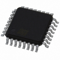
STLVD111BFR STMicroelectronics, STLVD111BFR Datasheet

STLVD111BFR
Specifications of STLVD111BFR
Available stocks
Related parts for STLVD111BFR
STLVD111BFR Summary of contents
Page 1
... Control Register. The purpose is to enable or power off each output clock channel and to select the clock input. The Order codes Temperature Part number range STLVD111BFR - °C May 2007 Programmable low voltage 1:10 differential LVDS clock driver BB STLVD111 is specifically designed, modelled and produced with low skew as the key goal ...
Page 2
Contents 1 Pin configuration . . . . . . . . . . . . . . . . . . . . . . . . . . . . . . . . . . . . ...
Page 3
Pin configuration Figure 1. Pin connections 3/19 ...
Page 4
Table 1. Pin description Pin n° 4/19 Symbol ...
Page 5
Maximum ratings Table 2. Absolute maximum ratings Symbol V Supply voltage CC V Input voltage I V Output voltage O I Driver short circuit current OSD ESD Electrostatic discharge (HBM 1.5KΩ, 100pF) Note: Absolute Maximum Ratings are those values ...
Page 6
Electrical characteristics Table 5. Driver electrical characteristics (T specified Note Symbol Parameter V Output differential voltage OD ΔV V magnitude change Offset voltage OS ΔV V magnitude change Output short circuit ...
Page 7
Table 7. Driver electrical characteristics (T specified Note Symbol Parameter V Output reference voltage BB I Power supply current CCD C Input capacitance IN C Output capacitance OUT V Logic input high threshold IH V Logic input low ...
Page 8
Specification of control register The STLVD111 is provided with a 11 bit shift register with a Serial In and a Control Register. The purpose is to enable or power of each output clock channel and to select the clock ...
Page 9
Table 13. Truth table All drivers enable CLK 0 CLK 0 CLK ...
Page 10
Diagram Figure 2. Logic diagram 10/19 ...
Page 11
Figure 3. Bank skew - t sk(b) 1. BANKSKEW is the magnitude of the time difference between outputs with a single driving input terminal Figure 4. Part to part skew - t 1. PART TO PART SKEW is the magnitude ...
Page 12
Figure 5. Pulse skew - t sk(P) 1. PULSE SKEW is the magnitude of the time difference between the high to low and low to high propagation delay times at an output. Figure 6. Voltage and current definition 12/19 (1) ...
Page 13
Figure 7. Test circuit and voltage definition for the differential output signal . Figure 8. Differential receiver to drive propagation delay and drive transition time waveforms 13/19 ...
Page 14
Figure 9. Set-Up, hold and the removal time, maximum frequency, minimum pulse width waveforms 14/19 ...
Page 15
Package mechanical data In order to meet environmental requirements, ST offers these devices in ECOPACK packages. These packages have a Lead-free second level interconnect. The category of second Level Interconnect is marked on the package and on the inner ...
Page 16
DIM. MIN 0.05 A2 1.35 B 0. 0° 16/19 TQFP32 MECHANICAL DATA mm. TYP MAX. 1.6 0.15 ...
Page 17
Tape & Reel TQFP32 MECHANICAL DATA mm. DIM. MIN. TYP A C 12 9.5 Bo 9.5 Ko 2.1 Po 3.9 P 11.9 inch MAX. MIN. TYP. 330 13.2 0.504 0.795 2.362 22.4 9.7 0.374 ...
Page 18
Revision history Table 14. Revision history Date Revision 30-May-2007 8 18/19 Changes Order codes has been updated and the document has been reformatted. ...
Page 19
... Information in this document is provided solely in connection with ST products. STMicroelectronics NV and its subsidiaries (“ST”) reserve the right to make changes, corrections, modifications or improvements, to this document, and the products and services described herein at any time, without notice. All ST products are sold pursuant to ST’s terms and conditions of sale. ...


